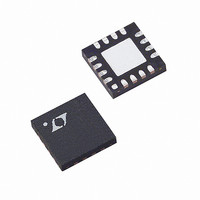
LTC5100EUF#TRPBF Linear Technology, LTC5100EUF#TRPBF Datasheet - Page 5

LTC5100EUF#TRPBF
Manufacturer Part Number
LTC5100EUF#TRPBF
Description
IC DRIVER VCSEL 3.2GBPS 16QFN
Manufacturer
Linear Technology
Type
Laser Diode Driverr
Datasheet
1.LTC5100EUF.pdf
(52 pages)
Specifications of LTC5100EUF#TRPBF
Data Rate
3.2Gbps
Number Of Channels
1
Voltage - Supply
3.135 V ~ 3.465 V
Current - Supply
54mA
Current - Modulation
12mA
Operating Temperature
-40°C ~ 85°C
Package / Case
16-QFN
Mounting Type
Surface Mount
Lead Free Status / RoHS Status
Lead free / RoHS Compliant
Available stocks
Company
Part Number
Manufacturer
Quantity
Price
temperature range, otherwise specifications are at T
resistor from SRC (Pin 14) to MODA (Pin 11); 50 , 1% load AC coupled to MODB (Pin 10); 10nF, 10% capacitor from SRC (Pin 14) to
V
PARAMETER
Bias Current Limit, I
Set Point Resolution
Set Point Range
Optical Power Limit
Overpower Limit
Underpower Limit
Safety Shutdown Response Time
FAULT Output, Open-Drain Mode, Flt_drv_mode = 0
Output Low Voltage
Output High Leakage Current
FAULT Output, Open-Drain Mode with 330 A Internal Pull Up, Flt_drv_mode = 1
Output Low Voltage
Output High Current
FAULT Output, Open-Drain Mode with 500 A Internal Pull Up, Flt_drv_mode = 2
Output Low Voltage
Output High Current
FAULT Output, Complementary Drive Mode, Flt_drv_mode = 3
Output High Voltage
Output Low Voltage
EN Input, Ib_gain or (Apc_gain in APC Mode) = 16, Im_gain = 4, Is_rng = 0, Im_rng = 0
Input Low Voltage
Input High Voltage
Input Low Current
Input High Current
Input Low Current
Input High Current
Transmit Enable Time
Transmit Re-Enable Time
Transmit Disable Time
Minimum Pulse Width Required to Clear
a Latched Fault
ELECTRICAL CHARACTERISTICS
SS
; Cml_en = 0, Lpc_en = 1, transmitter enabled, unless otherwise noted. Test circuit in Figure 5.
B(LIMIT)
CONDITIONS
Is_rng = 0
Is_rng = 1
Is_rng = 2
Is_rng = 3
Automatic Power Control Mode Only, Apc_en = 1
Expressed in % Over the Imd Set Point
Expressed in % Under the Imd Set Point
Time from the Fault Occurance to Reduction of
the Laser Bias Current to 10% of Nominal
I
V
I
V
I
V
I
I
En_polarity = 0 (EN Active Low), V
En_polarity = 0 (EN Active Low), V
En_polarity = 1 (EN Active High), V
En_polarity = 1 (EN Active High), V
Time from Active Transition on EN to 95% of
Nominal Laser Power and 95% of Full Modulation.
First Time Transmission is Enabled After Power
On or with Rapid_restart_en = 0
Time from Active Transition on EN to 95% of
Nominal Laser Power and 95% of Full Modulation.
When Transmission is Re-Enabled After the First
Time and with Rapid_restart_en = 1
Time from Inactive Transition on EN to 5% of
Nominal Laser Power
OL
OL
OL
OH
OL
FAULT
FAULT
FAULT
A
= 3.3mA
= 3.3mA
= 3.3mA
= 3.3mA
= –3.3mA
= 25 C; V
= 2.4V
= 2.4V
= 2.4V
The
DD
denotes the specifications which apply over the full operating
= V
DD(HS)
= 3.3V, I
EN
EN
EN
EN
= 0V
= V
= 0V
= V
S
DD
DD
= 24mA; I
M
= 12mA (I
MIN
2.4
10
2
MPP
–10 to 10
–10 to 10
–425
–280
TYP
–50
100
–10
100
18
27
36
50
10
10
= 24mA); 49.9 , 1%
7
9
1
LTC5100
MAX
0.4
0.4
0.4
0.4
0.8
10
sn5100 5100fs
UNITS
5
Bits
mA
mA
mA
mA
ms
ms
%
%
V
A
V
A
V
A
V
V
V
V
A
A
A
A
s
s
s


