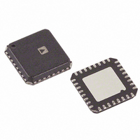
ADN2848ACP-32 Analog Devices Inc, ADN2848ACP-32 Datasheet - Page 6

ADN2848ACP-32
Manufacturer Part Number
ADN2848ACP-32
Description
IC DRVR LASER DIODE 3.3V 32LFCSP
Manufacturer
Analog Devices Inc
Type
Laser Diode Driver (Fiber Optic)r
Datasheet
1.ADN2848ACPZ-32-RL.pdf
(12 pages)
Specifications of ADN2848ACP-32
Number Of Channels
1
Rohs Status
RoHS non-compliant
Data Rate
1.25Gbps
Voltage - Supply
3 V ~ 3.6 V
Current - Supply
50mA
Current - Modulation
80mA
Current - Bias
100mA
Operating Temperature
-40°C ~ 85°C
Package / Case
32-VFQFN, CSP Exposed Pad
Mounting Type
Surface Mount
Operating Supply Voltage (min)
3V
Mounting
Surface Mount
Lead Free Status / RoHS Status
Not Compliant
ADN2848
PIN CONFIGURATION AND FUNCTION DESCRIPTIONS
Table 3. Pin Function Descriptions
Pin No.
1
2
3
4
5
6
7
8
9
10
11
12
13
14
15
16
17
18
19
20
21
22
23
24
25
26
27
28
29, 30
31
32
Mnemonic
LBWSET
ASET
ERSET
PSET
IMPD
IMPDMON
GND4
V
ERCAP
PAVCAP
V
DATAN
DATAP
GND1
CLKP
CLKN
CLKSEL
DEGRADE
FAIL
ALS
V
GND3
IMMON
IBMON
V
IMODN
GND2
IMODP
GND2
I
CCBIAS
BIAS
CC
CC
CC
CC
4
1
3
2
Description
Loop Bandwidth Select.
Alarm Threshold Set Pin.
Extinction Ratio Set Pin.
Average Optical Power Set Pin.
Monitor Photodiode Input.
Mirrored Current from Monitor Photodiode—Current Source.
Supply Ground.
Supply Voltage.
Extinction Ratio Loop Capacitor.
Average Power Loop Capacitor.
Supply Voltage.
Data Negative Differential Terminal.
Data Positive Differential Terminal.
Supply Ground.
Data Clock Positive Differential Terminal. This pin is used if CLKSEL = V
Clock Select (Active = V
DEGRADE Alarm Output.
FAIL Alarm Output.
Automatic Laser Shutdown.
Supply Voltage.
Supply Ground.
Bias Current Mirror Output—Current Source.
Supply Voltage.
Modulation Current Negative Output. Connect this pin via a matching resistor to V
Supply Ground.
Modulation Current Positive Output. Connect this pin to the laser diode.
Supply Ground.
Laser Diode Bias Current—Current Sink.
Connected to Vcc When DC-Coupled to Laser Diode; Connected to I
Diode—Current Sink.
Data Clock Negative Differential Terminal. This pin is used if CLKSEL = V
Modulation Current Mirror Output—Current Source.
IMPDMON 6
LBWSET 1
ERSET 3
GND4 7
ASET 2
PSET 4
IMPD 5
V
CC
4 8
CC
Figure 3. Pin Configuration
). This pin is used if data is clocked into chip.
Rev. A | Page 6 of 12
(Not to Scale)
ADN2848
PIN 1
INDICATOR
TOP VIEW
24 IBMON
23 IMMON
22 GND3
21 V
20 ALS
19 FAIL
18 DEGRADE
17 CLKSEL
CC
3
BIAS
CC
CC
When AC-Coupled to Laser
.
.
CC
.


