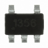
ZXLD1356ET5TA Diodes Zetex, ZXLD1356ET5TA Datasheet - Page 4

ZXLD1356ET5TA
Manufacturer Part Number
ZXLD1356ET5TA
Description
IC LED DRIVR WHITE BCKLGT TSOT-5
Manufacturer
Diodes Zetex
Type
Backlight, White LEDr
Datasheet
1.ZXLD1356ET5TA.pdf
(29 pages)
Specifications of ZXLD1356ET5TA
Topology
PWM, Step-Down (Buck)
Number Of Outputs
1
Internal Driver
Yes
Type - Primary
Automotive, Backlight
Type - Secondary
High Brightness LED (HBLED), White LED
Frequency
500kHz
Voltage - Supply
6 V ~ 60 V
Voltage - Output
60V
Mounting Type
Surface Mount
Package / Case
TSOT-23-5, TSOT-5, TSOP-5
Operating Temperature
-40°C ~ 125°C
Current - Output / Channel
550mA
Internal Switch(s)
Yes
Efficiency
97%
Lead Free Status / RoHS Status
Lead free / RoHS Compliant
Other names
ZXLD1356ET5TR
Available stocks
Company
Part Number
Manufacturer
Quantity
Price
Electrical Characteristics
Notes:
ZXLD1356
Document number: DS33470 Rev. 3 - 2
V
V
I
I
V
V
I
V
ΔV
V
V
V
R
I
R
I
D
DC
t
f
f
INQoff
INQon
SENSE
LXmean
LX(leak)
SS
LX
LXmax
Symbol
SU
SD
SENSE
SENSEHYS
REF
ADJ
ADJoff
ADJon
ADJ
LX
PWM(LF)
REF
ADJ
/ΔT
(*)
3. Static current of device is approximately 700 µA, see Graph, Page 17.
5. Ratio of maximum brightness to minimum brightness before shutdown V
4. 100% brightness corresponds to V
proportionally.
Internal regulator start-up threshold
Internal regulator shutdown threshold
Quiescent supply current with output off
Quiescent supply current with output switching
(Note 3)
Mean current sense threshold voltage
(Defines LED current setting accuracy)
Sense threshold hysteresis
I
Internal reference voltage
Temperature coefficient of V
External control voltage range on ADJ pin for DC
brightness control (Note 4)
DC voltage on ADJ pin to switch device from
active (on) state to quiescent (off) state
DC voltage on ADJ pin to switch device from
quiescent (off) state to active (on) state
Resistance between ADJ pin and V
Continuous LX switch current
LX switch ‘On’ resistance
LX switch leakage current
Duty cycle range of PWM signal applied to ADJ
pin during low frequency PWM dimming mode
Brightness control range
DC Brightness control range
Start up time
(See graphs for more details)
Operating frequency
(See graphs for more details)
Recommended maximum operating frequency
SENSE
pin input current
Parameter
(Test conditions: V
ADJ
= V
REF
ADJ(nom)
REF
= V
REF
IN
www.diodes.com
. Driving the ADJ pin above V
= 12V, T
4 of 29
ADJ pin grounded
ADJ pin floating,
L=68mH, 3 LEDs
f=360kHz
Measured on I
with respect to V
V
V
Measured on ADJ pin
with pin floating
V
V
0< V
V
@ I
PWM frequency
<300Hz PWM
amplitude =V
Measured on ADJ pin
Note 5
Time taken for output
current to reach 90% of
final value after voltage
on ADJ pin has risen
above 0.3V.
Requires external
capacitor 22nF.
ADJ pin floating
L=68mH (0.36V)
I
V
Driving 3 LEDs
amb
OUT
ADJ
SENSE
ADJ
ADJ
ADJ
LED
REF
LX
=0.55A @
= 25°C, unless otherwise specified.)
=1.25V; V
>V
=3.6V
ADJ
=1.25/0.25. V
falling
rising
=0.55A
Condition
=V
REF
< V
IN
+100mV
-0.2
REF
REF
IN
SENSE
REF
REF
=18V
IN
will increase the V
Diodes Incorporated
externally driven to 2.5V, ratio 10.1.
pin
A Product Line of
0.001
Min.
0.15
10.4
195
4.4
0.3
0.2
30
SENSE
1000:1
Typ.
4.85
1.25
0.25
4.75
14.2
200
±15
360
. threshold and output current
1.6
0.2
0.5
5:1
65
50
50
4
2
Max.
0.27
0.55
0.75
108
205
500
5.2
2.5
0.3
10
65
18
5
1
© Diodes Incorporated
ZXLD1356
December 2010
ppm/°C
Unit
kHz
kHz
mA
mV
ms
µA
µA
kΩ
µA
%
Ω
V
V
V
V
V
V
A


