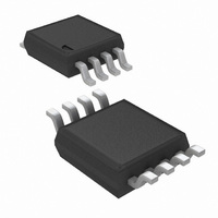
LM3401MM/NOPB National Semiconductor, LM3401MM/NOPB Datasheet - Page 3

LM3401MM/NOPB
Manufacturer Part Number
LM3401MM/NOPB
Description
IC LED DRIVER HIGH BRIGHT 8-MSOP
Manufacturer
National Semiconductor
Series
PowerWise®r
Type
HBLED Driverr
Datasheet
1.LM3401MMNOPB.pdf
(18 pages)
Specifications of LM3401MM/NOPB
Constant Current
Yes
Topology
PWM, Step-Down (Buck)
Number Of Outputs
1
Internal Driver
No
Type - Primary
General Purpose
Type - Secondary
High Brightness LED (HBLED)
Frequency
1.5MHz
Voltage - Supply
4.5 V ~ 35 V
Mounting Type
Surface Mount
Package / Case
8-MSOP, Micro8™, 8-uMAX, 8-uSOP,
Operating Temperature
-40°C ~ 125°C
Current - Output / Channel
1A
Internal Switch(s)
Yes
Efficiency
92%
Operating Supply Voltage (typ)
5/9/12/15/18/24V
Number Of Segments
1
Operating Temperature (min)
-40C
Operating Temperature (max)
125C
Operating Temperature Classification
Automotive
Package Type
MSOP
Pin Count
8
Mounting
Surface Mount
Power Dissipation
660mW
Operating Supply Voltage (min)
4.5V
Operating Supply Voltage (max)
35V
For Use With
LM3401EVAL - BOARD EVALUATION FOR LM3401
Lead Free Status / RoHS Status
Lead free / RoHS Compliant
Voltage - Output
-
Lead Free Status / Rohs Status
Compliant
Other names
LM3401MMTR
Available stocks
Company
Part Number
Manufacturer
Quantity
Price
Part Number:
LM3401MM/NOPB
Manufacturer:
NS/国半
Quantity:
20 000
SYSTEM
DRIVER
ΔV
SNS
Absolute Maximum Ratings
If Military/Aerospace specified devices are required,
please contact the National Semiconductor Sales Office/
Distributors for availability and specifications.
Electrical Characteristics
apply over the junction temperature (T
limits are guaranteed through test, design, or statistical correlation. Typical values represent the most likely parametric norm at
T
Note 1: Absolute Maximum Ratings indicate limits beyond which damage may occur to the device. Operating Ratings indicate conditions for which the device is
intended to be functional, but do not guarantee specific performance limits. For guaranteed specifications, see Electrical Characteristics.
Note 2: The human body model is a 100 pF capacitor discharged through a 1.5 kΩ resistor into each pin.
Note 3: The maximum allowable power dissipation is a function of the maximum junction temperature, T
and the ambient temperature, T
maximum power dissipation of 0.66W is determined using T
θ
Note 4: All room temperature limits are 100% production tested. All limits at temperature extremes are guaranteed through correlation using standard Statistical
Quality Control (SQC) methods. All limits are used to calculate Average Outgoing Quality Level (AOQL).
Note 5: IQ specifies the current into the VIN pin and applies to non-switching operation.
VIN
CS
SNS
ILIM
DIM
HYS
Storage Temperature
JA
J
Ton_min
Symbol
V
REF
UVLO
= 25°C, and are provided for reference purposes only (Note 4).
spec is based on a JEDEC standard 4-layer board.
V
T
CL_OFF
T
V
I
I
R
V
I
V
I
HYS
SNS
ILIM
HYS_MU
REF
I
DLY
HG
DIM
DIM
HG
HG
Q
ZC
/ ΔV
IN
Parameter
Reference Voltage
Line regulation
Operating VIN Current (Note 5)
Hysteresis Pin Source Current
SNS Comparator Hysteresis Multiplier
SNS Comparator to HG Delay
DIM to HG Delay
ILIM Pin Sink Current
Current Limit Comparator Offset
Zero Cross Comparator Threshold
DIM Threshold Voltage
Hysteresis
SNS pin Bias Current
UVLO threshold
Hysteresis
Minimum on-time
Gate Drive Resistance
Driver Output Current
HG on voltage
A
. The maximum allowable power dissipation at any ambient temperature is calculated using: P
J
) range of -40°C to +125°C. Unless otherwise stated, V
-65°C to +150°C
Specifications in standard type are for T
-0.3V to 36V
-2.0V to 36V
-0.3V to 36V
-0.3V to 36V
(Note 1)
-0.3V to 8V
-0.3V to 4V
A
= 25°C, θ
JA
Conditions
5V < VIN < 35V
HYS pin = 50 mV to 500 mV
HYS pin = 250 mV
SNS rising
DIM rising
Measured at CS pin
V
Vin rising
Source Current = 100 mA
Sink Current = 100 mA
Source, HG = VIN -2.5V
Sink, HG = VIN -2.5V
Referenced to VIN, steady state voltage
SNS
= 151°C/W, and T
= 200 mV
3
Operating Ratings
Lead Temperature
ESD Rating (Note 2)
Human Body Model
VIN
Junction Temperature Range
Thermal Resistance θ
Power Dissispation (Note 3)
Vapor Phase (60sec)
Infrared (15sec)
J_MAX
= 125°C. θ
J_MAX
J
= 25°C only, and limits in boldface type
JA
, the junction-to-ambient thermal resistance, θ
will vary with board size and copper area. The
JA
(Note 3)
IN
= 24V. Minimum and Maximum
0.168
1.85
(Note 1)
Min
188
-4.2
-10
-70
15
4
D_MAX
= (T
0.002
-130
1.05
0.20
10.5
0.41
0.33
Typ
-4.7
200
286
300
150
5.5
2.0
4.3
0.5
5.3
20
46
69
0
J_MAX
-40°C to +125°C
- T
4.5V to 35V
0.224
www.national.com
-200
Max
2.25
4.48
-5.5
212
120
+10
780
25
80
A
151°C/W
8
)/θ
JA
0.66W
215°C
2.5kV
220C
. The
Units
mV/V
mV
mA
mV
mV
mV
JA
µA
µA
nA
ns
ns
ns
V
V
V
Ω
Ω
A
A
V
-
,


