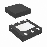
LM3410XSD/NOPB National Semiconductor, LM3410XSD/NOPB Datasheet - Page 14

LM3410XSD/NOPB
Manufacturer Part Number
LM3410XSD/NOPB
Description
IC LED DRVR WT/OLED BCKLGT 6-LLP
Manufacturer
National Semiconductor
Series
PowerWise®r
Type
Backlight, OLED, White LEDr
Datasheet
1.LM3410XMFNOPB.pdf
(32 pages)
Specifications of LM3410XSD/NOPB
Constant Current
Yes
Topology
PWM, SEPIC, Step-Up (Boost)
Number Of Outputs
1
Internal Driver
Yes
Type - Primary
Automotive, Backlight, Flash/Torch
Type - Secondary
High Brightness LED (HBLED), OLED, White LED
Frequency
1.2MHz ~ 2MHz
Voltage - Supply
2.7 V ~ 5.5 V
Voltage - Output
3 V ~ 24 V
Mounting Type
Surface Mount
Package / Case
6-LLP
Operating Temperature
-40°C ~ 125°C
Current - Output / Channel
2.8A
Internal Switch(s)
Yes
Efficiency
88%
For Use With
LM3410XSDLEDEV - BOARD EVAL LM3410 BOOST LLP
Lead Free Status / RoHS Status
Lead free / RoHS Compliant
Other names
LM3410XSDTR
www.national.com
Calculating Efficiency, and Junction
Temperature
We will talk more about calculating proper junction tempera-
ture with relative certainty in a moment. For now we need to
describe how to calculate the junction temperature and clarify
some common misconceptions.
A common error when calculating R
package is the only variable to consider.
R
•
•
•
•
•
Another common error when calculating junction temperature
is to assume that the top case temperature is the proper tem-
perature when calculating R
impedance of all six sides of a package, not just the top side.
This document will refer to a thermal impedance called
top case temperature. This will allow one to calculate the
junction temperature with a thermal sensor connected to the
top case.
The complete LM3410 Boost converter efficiency can be cal-
culated in the following manner.
Power loss (P
converter, switching and conduction. Conduction losses usu-
ally dominate at higher output loads, where as switching
losses remain relatively fixed and dominate at lower output
loads.
Losses in the LM3410 Device: P
Where P
Conversion ratio of the Boost Converter with conduction loss
elements inserted:
Where
R
θJA
DCR
Input Voltage, Output Voltage, Output Current, R
Ambient temperature & air flow
Internal & External components power dissipation
Package thermal limitations
PCB variables (copper weight, thermal via’s, layers
component placement)
represents a thermal impedance associated with just the
[variables]:
= Inductor series resistance
Q
= quiescent operating power loss
LOSS
) is the sum of two types of losses in the
θJC
. R
LOSS
θJC
θJA
= P
represents the thermal
is to assume that the
COND
+ P
SW
DS(ON)
+ P
Q
.
14
One can see that if the loss elements are reduced to zero, the
conversion ratio simplifies to:
And we know:
Therefore:
Calculations for determining the most significant power loss-
es are discussed below. Other losses totaling less than 2%
are not discussed.
A simple efficiency calculation that takes into account the
conduction losses is shown below:
The diode, NMOS switch, and inductor DCR losses are in-
cluded in this calculation. Setting any loss element to zero will
simplify the equation.
V
can be obtained from the manufacturer’s Electrical Charac-
teristics section of the data sheet.
The conduction losses in the diode are calculated as follows:
Depending on the duty cycle, this can be the single most sig-
nificant power loss in the circuit. Care should be taken to
choose a diode that has a low forward voltage drop. Another
concern with diode selection is reverse leakage current. De-
pending on the ambient temperature and the reverse voltage
across the diode, the current being drawn from the output to
the NMOS switch during time D could be significant, this may
increase losses internal to the LM3410 and reduce the overall
efficiency of the application. Refer to Schottky diode
manufacturer’s data sheets for reverse leakage specifica-
tions, and typical applications within this data sheet for diode
selections.
Another significant external power loss is the conduction loss
in the input inductor. The power loss within the inductor can
be simplified to:
D
is the forward voltage drop across the Schottky diode. It
P
DIODE
= V
D
x I
LED


