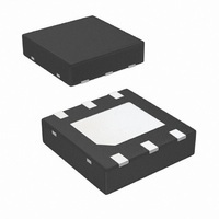
LM3410XSD/NOPB National Semiconductor, LM3410XSD/NOPB Datasheet - Page 4

LM3410XSD/NOPB
Manufacturer Part Number
LM3410XSD/NOPB
Description
IC LED DRVR WT/OLED BCKLGT 6-LLP
Manufacturer
National Semiconductor
Series
PowerWise®r
Type
Backlight, OLED, White LEDr
Datasheet
1.LM3410XMFNOPB.pdf
(32 pages)
Specifications of LM3410XSD/NOPB
Constant Current
Yes
Topology
PWM, SEPIC, Step-Up (Boost)
Number Of Outputs
1
Internal Driver
Yes
Type - Primary
Automotive, Backlight, Flash/Torch
Type - Secondary
High Brightness LED (HBLED), OLED, White LED
Frequency
1.2MHz ~ 2MHz
Voltage - Supply
2.7 V ~ 5.5 V
Voltage - Output
3 V ~ 24 V
Mounting Type
Surface Mount
Package / Case
6-LLP
Operating Temperature
-40°C ~ 125°C
Current - Output / Channel
2.8A
Internal Switch(s)
Yes
Efficiency
88%
For Use With
LM3410XSDLEDEV - BOARD EVAL LM3410 BOOST LLP
Lead Free Status / RoHS Status
Lead free / RoHS Compliant
Other names
LM3410XSDTR
www.national.com
Absolute Maximum Ratings
If Military/Aerospace specified devices are required,
please contact the National Semiconductor Sales Office/
Distributors for availability and specifications.
Electrical Characteristics
junction temperature (T
correlation. Typical values represent the most likely parametric norm at T
V
Note 1: Absolute Maximum Ratings indicate limits beyond which damage to the device may occur. Operating Ratings indicate conditions for which the device is
intended to be functional, but does not guarantee specific performance limits. For guaranteed specifications and conditions, see the Electrical Characteristics.
Note 2: Thermal shutdown will occur if the junction temperature exceeds the maximum junction temperature of the device.
Note 3: Applies for packages soldered directly onto a 3” x 3” PC board with 2oz. copper on 4 layers in still air.
Note 4: The human body model is a 100 pF capacitor discharged through a 1.5 kΩ resistor into each pin. Test method is per JESD22-A114.
Note 5: Do not allow this pin to float or be greater than V
V
SW Voltage
FB Voltage
DIM Voltage
ESD Susceptibility
Human Body Model
Junction Temperature
ΔV
IN
Symbol
R
IN
V
UVLO
D
D
= 5V, unless otherwise indicated under the Conditions column.
DS(ON)
F
V
DIM_H
I
T
SU
I
θ
θ
FB
I
I
DIM
MAX
I
SW
FB
MIN
CL
SW
JA
JC
SD
FB
Q
/V
IN
Feedback Voltage
Feedback Voltage Line Regulation
Feedback Input Bias Current
Switching Frequency
Maximum Duty Cycle
Minimum Duty Cycle
Switch On Resistance
Switch Current Limit
Start Up Time
Quiescent Current (switching)
Quiescent Current (shutdown)
Undervoltage Lockout
Shutdown Threshold Voltage
Enable Threshold Voltage
Switch Leakage
Dimming Pin Current
Junction to Ambient
0 LFPM Air Flow
Junction to Case
Thermal Shutdown Temperature
(Note
J
(Note
) range of -40°C to 125°C. Minimum and Maximum limits are guaranteed through test, design, or statistical
4)
2)
Parameter
(Note
(Note
3)
3)
-0.5V to 26.5V
Limits in standard type are for T
IN
-0.5V to 3.0V
-0.5V to 7.0V
(Note
+0.3V.
-0.5V to 7V
(Note
150°C
1)
2)
2kV
V
LM3410-X
LM3410-Y
LM3410-X
LM3410-Y
LM3410-X
LM3410-Y
SOT23-5 and eMSOP-8
LLP-6
LM3410-X V
LM3410-Y V
All Options V
V
V
V
Sink/Source
LLP-6 and eMSOP-8 Package
SOT23-5 Package
LLP-6 and eMSOP-8 Package
SOT23-5 Package
IN
IN
IN
SW
= 2.7V to 5.5V
Rising
Falling
= 24V
4
Operating Ratings
Storage Temp. Range
Soldering Information
V
V
V
Junction Temperature Range
Power Dissipation
(Internal) SOT23-5
IN
DIM
SW
Infrared/Convection Reflow (15sec)
FB
FB
DIM
Conditions
J
= 0.25
= 0.25
(Note
= 25°C, and are provided for reference purposes only.
= 0V
J
= 25°C only; limits in boldface type apply over the
5)
1200
(Note
Min
178
360
2.1
1.7
1.8
88
90
-
-
-
-
-
-
-
-
-
-
-
-
-
-
-
-
-
-
1)
1600
0.06
2.80
Typ
190
525
170
190
100
118
165
0.1
7.0
3.4
2.3
1.9
1.0
92
95
20
80
80
18
60
5
2
-
-
-40°C to 125°C
-65°C to 150°C
2.7V to 5.5V
2000
Max
2.65
202
680
330
350
3V to 24V
0.4
11
0V to V
1
7
-
-
-
-
-
-
-
-
-
-
-
-
-
-
-
-
-
400 mW
220°C
Units
°C/W
°C/W
%/V
kHz
mΩ
mV
mA
IN
µA
nA
µA
nA
µs
°C
%
%
A
V
V


