LM3530UME-40/NOPB National Semiconductor, LM3530UME-40/NOPB Datasheet
LM3530UME-40/NOPB
Specifications of LM3530UME-40/NOPB


Related parts for LM3530UME-40/NOPB


LM3530UME-40/NOPB Summary of contents
Page 1
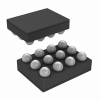
... The LM3530 is available in a tiny 12-bump (1.6mm × 1.2mm × 0.425mm) micro SMD package and operates over the −40° +85°C temperature range. Typical Application Circuit © 2011 National Semiconductor Corporation LM3530 Features ■ Drives LED’s in series ■ ...
Page 2
... NOPB micro SMD LM3530UMX-25A 12-Bump NOPB micro SMD LM3530UME-40 12-Bump NOPB micro SMD LM3530UMX-40 12-Bump NOPB micro SMD LM3530UME-40B 12-Bump NOPB micro SMD LM3530UMX-40B 12-Bump NOPB micro SMD www.national.com 30086602 Supplied As Lead Free? (2 lines: first line (XX) is date code and die run code, second line is ...
Page 3
Pin Descriptions/Functions Pin Name Description C3 IN Input Voltage Connection. Connect a 2.7V to 5.5V supply to IN and bypass to GND with a 2.2µF or greater ceramic capacitor. D2 OVP Output Voltage Sense Connection for Over-Voltage Sensing. Connect OVP ...
Page 4
... IN Resistance (T Internally Limited +150°C ESD Caution Notice −65°C to +150°C National Semiconductor recommends that all integrated cir- cuits be handled with appropriate ESD precautions. Failure to (Note 3) observe proper ESD handling techniques can result in dam- age to the device. 2.0kV (Note ...
Page 5
Symbol Parameter Logic Thresholds - Logic Low V HWEN Logic Thresholds - Logic High T Thermal Shutdown SD Hysteresis RALS1, ALS Input Internal Pull-down RALS2 Resistors Logic Voltage Specifications (SCL, SDA, PWM, INT) V Input Logic Low IL V Input ...
Page 6
... Note 2: All voltages are with respect to the potential at the GND pin. Note 3: For detailed soldering specifications and information, please refer to National Semiconductor Application Note 1112: Micro SMD Wafer Level Chip Scale Package (AN-1112), available at www.national.com. Note 4: Internal thermal shutdown circuitry protects the device from permanent damage. Thermal shutdown engages =+125° ...
Page 7
Timing Diagrams FIGURE C-Compatible Timing FIGURE 2. Simple Enable/Disable Timing 7 30086603 30086604 www.national.com ...
Page 8
Typical Performance Characteristics C = 1µ 1µ TDK VLF5012ST-100M1R0, (R OUT IN Efficiency FULL_SCALE Efficiency FULL_SCALE Efficiency vs I LED www.national.com V = 3.6V, LEDs are OVSRWAC1R6 from ...
Page 9
LED Current vs V (19mA Full-Scale Setting) IN Internal ALS Resistor +25° ALS Resistor Select Register = 0x44 Internal ALS Resistor −40° ALS Resistor Select Register = 0x44 ...
Page 10
Over Voltage Protection vs V NFET Switch On-Resistance vs V Simple Enable Time vs V www.national.com (V Rising) IN OUT 30086660 IN 30086678 IN 30086680 10 Max Duty Cycle 30086676 Switching Frequency 30086677 Simple ...
Page 11
LED PWM (50% duty cycle, I Full Scale = 19mA) LED Ramp Rate (Exponential) (2.048ms/step up and down) Channel 2: SDA (5V/div) Channel 3: ILED (10mA/div) Time Base (100ms/div) Ramp Rate (Exponential) (8.192ms/step up and down) Channel ...
Page 12
Ramp Rate (Exponential) (32.768ms/step up and down) Channel 2: SDA (5V/div) Channel 3: ILED (10mA/div) Time Base (2s/div) Startup Plot (V = 3.6V, ILED = 19mA 22µH, Ramp Rate = 8µs/step) IN Channel 1: IIN (200mA/div) Channel 3: ...
Page 13
Operational Description The LM3530 utilizes an asynchronous step-up, current mode, PWM controller and regulated current sink to provide an effi- cient and accurate LED current for white LED bias. The device powers a single series string of LEDs with output ...
Page 14
ALS AVERAGING TIME The ALS Averaging Time is the time over which the Averager block collects samples from the A/D converter and then av- erages them to pass to the discriminator block (see 3). Ambient light sensor samples are averaged ...
Page 15
FIGURE 5. Averager Calculation FIGURE 6. Brightness Zone Change Examples 15 30086685 30086686 www.national.com ...
Page 16
FIGURE 7. Ambient Light Input to Backlight Transition ZONE BOUNDARY SETTINGS Registers 0x60, 0x61, 0x62, and 0x63 set the 4 zone bound- aries (thresholds) for the ALS inputs. These 4 zone bound- aries create 5 brightness zones which map over ...
Page 17
Zone Boundary registers, and V is typically 7mV. HYST 2. If the last zone transition was from high to low then the trip point (V ) will be V TRIP ZONE_BOUNDARY Figure 9 details how the LM3530's ...
Page 18
TABLE 1. Ideal Zone Boundary Settings with Hysteresis (Lower 5 Codes) Zone Boundary Code 0x00 0x01 0x02 0x03 0x04 LED CURRENT CONTROL The LED current function of the Full Scale Current, the Brightness Code, and the PWM ...
Page 19
EXPONENTIAL OR LINEAR BRIGHTNESS MAPPING MODES With bit [1] of the General Configuration Register set to 0 (de- fault) exponential mapping is selected and the code in the Brightness Control Register corresponds to the Full-Scale LED current percentages in Table ...
Page 20
TABLE 2. I BRT Data % Full-Scale BRT Data (Hex) Current 0x00 0.00% 0x01 0.080% 0x02 0.086% 0x03 0.094% 0x04 0.102% 0x05 0.109% 0x06 0.117% 0x07 0.125% 0x08 0.133% 0x09 0.141% 0x0A 0.148% 0x0B 0.156% 0x0C 0.164% 0x0D 0.172% 0x0E ...
Page 21
BRT Data % Full-Scale BRT Data (Hex) Current (Hex) 0x1D 0.422% 0x3D 0x1E 0.445% 0x3E 0x1F 0.469% 0x3F TABLE 3. I BRT Data % Full-Scale BRT Data (Hex) Current (Hex) (Linear) 0x00 0.00% 0x20 0x01 0.79% 0x21 0x02 1.57% 0x22 ...
Page 22
BRT Data % Full-Scale (Hex) Current (Linear) 0x16 17.32% 0x17 18.11% 0x18 18.90% 0x19 19.69% 0x1A 20.47% 0x1B 21.26% 0x1C 22.05% 0x1D 22.83% 0x1E 23.62% 0x1F 24.41% SIMPLE ENABLE DISABLE WITH PWM CURRENT CONTROL With bits [7 and 5] of ...
Page 23
Ambient Light Boundaries (ZB0 – ZB3) pro- grammed through the four (8-bit) Zone Boundary Registers. These zone boundaries define 5 ambient brightness zones (Figure 4). Each zone corresponds to a programmable bright- ness setting which is programmable through the ...
Page 24
Referring to Figure 14, initially the Averager is loaded with Zone takes 2 averaging periods for the LM3530 to change to the new zone. After the ALS1 voltage remains at 437.5mV for two averaging periods (end of ...
Page 25
INTERRUPT OUTPUT INT is an open-drain output which pulls low when the Ambient Light Sensing circuit has transitioned to a new ambient bright- ness zone. When a read-back of the ALS Information Register is done INT is reset to the ...
Page 26
I 2 C-Compatible Interface START AND STOP CONDITION The LM3530 is controlled via an I START and STOP conditions classify the beginning and the end of the session. A START condition is defined as SDA transitioning from ...
Page 27
Register Descriptions Register Name Function 1. Simple Interface Enable 2. PWM Polarity 3. PWM enable General Configuration 4. Full-Scale Current Selection 5. Brightness Mapping Mode Select Device Enable 1. ALS Current Control Enable 2. ALS Input ...
Page 28
GENERAL CONFIGURATION REGISTER (GP) The General Configuration Register (address 0x10) is de- scribed in Figure 18 and Table 5. TABLE 5. General Configuration Register Description (0x10) Bit 7 Bit 6 (PWM Simple (PWM Enable Polarity Simple 0 = ...
Page 29
TABLE 6. ALS Configuration Register Description (0x20) Bit 7 Bit 6 Bit 5 ALS Input ALS Input Select Select N The Average of ALS1 and ALS2 is used to control the LED brightness 01 = ALS1 is used ...
Page 30
TABLE 8. ALS Zone Information Register Description (0x40) Bit 7 Bit 6 Bit 5 Bit 4 N/A N/A N/A N/A ALS RESISTOR SELECT REGISTER The ALS Resistor Select Register configures the internal re- sistance from either the ALS1 or ALS2 ...
Page 31
TABLE 10. Brightness Control Register Description (0xA0) Bit 7 Bit 6 Bit 5 N/A Data (MSB) Data Exponential Mapping (see FIX) 0000000 = LEDs Off 0000001 = 0.08% of Full Scale : : : 1111111 = 100% of Full Scale ...
Page 32
ZONE BOUNDARY REGISTER The Zone Boundary Registers are programmed with the am- bient light sensing zone boundaries. The default values are set at 20% (200mV), 40% (400mV), 60% (600mV), and 80% www.national.com (800mV) of the full-scale ALS input voltage range ...
Page 33
ZONE TARGET REGISTERS The Zone Target Registers contain the LED brightness data that corresponds to the current active ALS zone. The default values for these registers and their corresponding percentage of full-scale current for both linear and exponential brightness is ...
Page 34
TABLE 11. Zone Boundary and Zone Target Default Mapping Zone Boundary (Default) Boundary 0, Active ALS input is less than 200 mV Boundary 1, Active ALS input is between 200 mV and 400 mV Boundary 2, Active ALS input is ...
Page 35
Applications Information LED CURRENT SETTING/MAXIMUM LED CURRENT The maximum LED current is restricted by the following fac- tors: the maximum duty cycle that the boost converter can achieve, the peak current limitations, and the maximum out- put voltage. MAXIMUM DUTY ...
Page 36
Manufacturer Part Number TDK VLF3014ST-100MR82 TDK VLF3010ST-220MR34 TDK VLF3010ST-100MR53 TDK VLF4010ST-100MR80 TDK VLS252010T-100M Coilcraft LPS3008-103ML Coilcraft LPS3008-223ML Coilcraft LPS3010-103ML Coilcraft LPS3010-223ML Coilcraft XPL2010-103ML Coilcraft EPL2010-103ML TOKO DE2810C-1117AS-100M DIODE SELECTION The diode connected between SW and OUT must be a Schot- ...
Page 37
FIGURE 26. LM3530's Boost Converter Showing Pulsed Voltage at SW (High dV/dt) and Current Through Schottky and C The following lists the main (layout sensitive) areas of the LM3530 in order of decreasing importance: Output Capacitor • Schottky Cathode to ...
Page 38
Schottky Diode Placement The Schottky diode is in the path of the inductor current dis- charge result the Schottky diode sees a high current step from each time the switch turns off and the PEAK ...
Page 39
FIGURE 27. Input RLC Network 39 30086628 www.national.com ...
Page 40
Example Layouts The following three figures show example layouts which apply the required proper layout guidelines. These figures should be used as guides for laying out the LM3530's circuit. www.national.com FIGURE 28. Layout Example #1 FIGURE 29. Layout Example #2 ...
Page 41
FIGURE 30. Layout Example #3 TABLE 15. Application Circuit Component List Compon- Manufact- Part Number ent urer L TDK VLF3014ST- 100MR82 COUT Murata GRM21BR71 H105KA12 CIN Murata GRM188B31 A225KE33 D1 Diodes Inc. B0540WS ALS1 Avago APDS-9005 ALS2 Avago APDS-9005 300866a3 ...
Page 42
Physical Dimensions X1 = 1.215 mm (±0.1 mm 1.615 mm (±0.1 mm 0.425 mm www.national.com inches (millimeters) unless otherwise noted 12-Bump Ultra Thin Micro SMD Package For Ordering, Refer to Ordering Information Table NS Package Number ...
Page 43
Notes 43 www.national.com ...
Page 44
... For more National Semiconductor product information and proven design tools, visit the following Web sites at: www.national.com Products Amplifiers www.national.com/amplifiers Audio www.national.com/audio Clock and Timing www.national.com/timing Data Converters www.national.com/adc Interface www.national.com/interface LVDS www.national.com/lvds Power Management www.national.com/power Switching Regulators www.national.com/switchers LDOs www.national.com/ldo LED Lighting www ...