LM2759SD/NOPB National Semiconductor, LM2759SD/NOPB Datasheet - Page 10
LM2759SD/NOPB
Manufacturer Part Number
LM2759SD/NOPB
Description
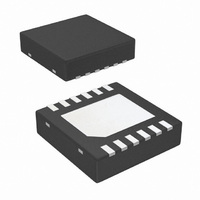
IC LED DRIVER PHOTO FLASH 12-LLP
Manufacturer
National Semiconductor
Series
PowerWise®r
Type
Photo Flash LED (I²C Interface)r
Datasheet
1.LM2759SDNOPB.pdf
(14 pages)
Specifications of LM2759SD/NOPB
Constant Current
Yes
Topology
Switched Capacitor (Charge Pump)
Number Of Outputs
1
Internal Driver
Yes
Type - Primary
Flash/Torch
Frequency
700kHz ~ 1.3MHz
Voltage - Supply
*
Voltage - Output
2 V ~ 4 V
Mounting Type
Surface Mount
Package / Case
12-LLP
Operating Temperature
-30°C ~ 85°C
Current - Output / Channel
1A
Internal Switch(s)
Yes
Efficiency
90%
Led Driver Application
Camera Flash In Mobile Phones, Flash For Digital Cameras
No. Of Outputs
1
Output Current
1A
Output Voltage
5.1V
Input Voltage
2.7V To 5.5V
Rohs Compliant
Yes
Lead Free Status / RoHS Status
Lead free / RoHS Compliant
Other names
LM2759SDTR
Available stocks
Company
Part Number
Manufacturer
Quantity
Price
Company:

Part Number:
LM2759SD/NOPB
Manufacturer:
National Semiconductor
Quantity:
1 790


www.national.com
data has to be followed by an acknowledge bit. The acknowl-
edge related clock pulse is generated by the master. The
master releases the SDA line (HIGH) during the acknowledge
clock pulse. The LM2759 pulls down the SDA line during the
9th clock pulse, signifying an acknowledge. The LM2759 gen-
erates an acknowledge after each byte is received.
After the START condition, the I
dress. This address is seven bits long followed by an eighth
I
The chip address for LM2759 is 1010011, or 53h.
INTERNAL REGISTERS
2
C COMPATIBLE CHIP ADDRESS
ack = acknowledge (SDA pulled down by either master or slave)
2
C master sends a chip ad-
id = chip address, 53h for LM2759
FIGURE 3. Write Cycle
30069309
30069308
30069305
30069306
30069307
w = write (SDA = "0")
r = read (SDA = "1")
10
bit which is a data direction bit (R/W). The LM2759 address
is 53h. For the eighth bit, a “0” indicates a WRITE and a “1”
indicates a READ. The second byte selects the register to
which the data will be written. The third byte contains data to
write to the selected register.
GENERAL PURPOSE REGISTER AND STROBE INHIBIT
FUNCTION
The general purpose register (x10) is used set the mode of
operation for the LM2759. The selectable operating modes
using the lower 4 bits in the general purpose register are listed
in the table below.
The Strobe Input Pin can be disabled via I
signals into this pin when desired. This function is implement-
ed through bit 3 of the General Purpose Register (See table
below). In the default state, input signals on the Strobe Input
are enabled. (Bit3 = “0”, inputs into the Strobe Pin are not
inhibited).
General Purpose
Register
Flash Current
Register
Torch Current
Register
Flash Timeout
Duration Register
Bit3
X
X
X
X
1
Register
Bit2
X
X
X
0
1
General Purpose Register (Reg x10)
Bit1
X
X
0
1
0
Bit0
Internal Hex
0
1
1
1
X
Address
C0h
10h
B0h
A0h
Inhibit Inputs into the Strobe Pin
Indicator (Lowest Torch Level)
Shutdown
Power On Value
2
Mode
C to ignore external
Torch
(lowest 4 bits)
Flash
30069312
0000
1010
0111
1011
Related parts for LM2759SD/NOPB
Image
Part Number
Description
Manufacturer
Datasheet
Request
R

Part Number:
Description:
National Semiconductor [8-Bit D/A Converter]
Manufacturer:
National Semiconductor
Datasheet:
Part Number:
Description:
National Semiconductor [Media Coprocessor]
Manufacturer:
National Semiconductor
Datasheet:
Part Number:
Description:
Digitally Controlled Tone and Volume Circuit with Stereo Audio Power Amplifier, Microphone Preamp Stage and National 3D Sound
Manufacturer:
National Semiconductor
Datasheet:
Part Number:
Description:
Digitally Controlled Tone and Volume Circuit with Stereo Audio Power Amplifier, Microphone Preamp Stage and National 3D Sound
Manufacturer:
National Semiconductor
Datasheet:
Part Number:
Description:
AC97 Rev 2 Codec with Sample Rate Conversion and National 3D Sound
Manufacturer:
National Semiconductor
Part Number:
Description:
Manufacturer:
National Semiconductor
Datasheet:
Part Number:
Description:
Manufacturer:
National Semiconductor
Datasheet:
Part Number:
Description:
General Purpose, Low Voltage, Low Power, Rail-to-Rail Output Operational Amplifiers
Manufacturer:
National Semiconductor
Datasheet:
Part Number:
Description:
8-bit 20 MSPS flash A/D converter.
Manufacturer:
National Semiconductor
Datasheet:
Part Number:
Description:
Low Noise Quad Operational Amplifier
Manufacturer:
National Semiconductor
Datasheet:
Part Number:
Description:
Quad Differential Line Receivers
Manufacturer:
National Semiconductor
Datasheet:
Part Number:
Description:
Quad High Speed Trapezoidal? Bus Transceiver
Manufacturer:
National Semiconductor
Datasheet:
Part Number:
Description:
Dual Line Receiver
Manufacturer:
National Semiconductor
Datasheet:
Part Number:
Description:
TTL to 10k ECL Level Translator with Latch
Manufacturer:
National Semiconductor
Datasheet: