LM2759SD/NOPB National Semiconductor, LM2759SD/NOPB Datasheet - Page 9
LM2759SD/NOPB
Manufacturer Part Number
LM2759SD/NOPB
Description
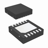
IC LED DRIVER PHOTO FLASH 12-LLP
Manufacturer
National Semiconductor
Series
PowerWise®r
Type
Photo Flash LED (I²C Interface)r
Datasheet
1.LM2759SDNOPB.pdf
(14 pages)
Specifications of LM2759SD/NOPB
Constant Current
Yes
Topology
Switched Capacitor (Charge Pump)
Number Of Outputs
1
Internal Driver
Yes
Type - Primary
Flash/Torch
Frequency
700kHz ~ 1.3MHz
Voltage - Supply
*
Voltage - Output
2 V ~ 4 V
Mounting Type
Surface Mount
Package / Case
12-LLP
Operating Temperature
-30°C ~ 85°C
Current - Output / Channel
1A
Internal Switch(s)
Yes
Efficiency
90%
Led Driver Application
Camera Flash In Mobile Phones, Flash For Digital Cameras
No. Of Outputs
1
Output Current
1A
Output Voltage
5.1V
Input Voltage
2.7V To 5.5V
Rohs Compliant
Yes
Lead Free Status / RoHS Status
Lead free / RoHS Compliant
Other names
LM2759SDTR
Available stocks
Company
Part Number
Manufacturer
Quantity
Price
Company:

Part Number:
LM2759SD/NOPB
Manufacturer:
National Semiconductor
Quantity:
1 790


Application Information
CIRCUIT DESCRIPTION
The LM2759 is an adaptive CMOS charge pump with gains
of 1x, 1.5x, and 2x, optimized for driving Flash LEDs in cam-
era phones and other portable applications. It provides a
constant current of up to 1A (typ.) for Flash mode and 180 mA
(typ.) for Torch mode.
The LM2759 has selectable modes including Flash, Torch,
Indicator and Shutdown. Flash mode for the LM2759 can also
be enabled via the Strobe input pin. The LED is driven from
V
and operating modes are programmed via an I
interface. The LM2759 adaptively selects the next highest
gain mode when needed to maintain the programmed LED
current level.
To prevent a high battery load condition during a simultane-
ous RF PA transmission and Flash event, LM2759 has a
Flash interrupt pin (TX) to reduce the LED current to the pro-
grammed Torch current level for the duration of the RF PA
transmission pulse.
CHARGE PUMP AND GAIN TRANSITIONS
The input to the 1x, 1.5x, 2x charge pump is connected to the
V
is connected to the V
voltage is less than 4.7V (typ.), the output voltage is approx-
imately equal to the input voltage. When the input voltage is
over 4.7V (typ.) the output voltage is regulated to 4.7V (typ.).
In 1.5x mode, the output voltage is regulated to 4.7V (typ.)
over entire input voltage range. For the gain of 2x, the output
voltage is regulated to 5.1V (typ.). When under load, the volt-
age at V
while the charge pump is still in closed loop operation. This is
due to the load regulation topology of the LM2759.
The charge pump’s gain is selected according to the head-
room voltage across the current sink of LM2759. When the
headroom voltage V
350 mV (typ.) the charge pump gain transitions to the next
available higher gain mode. Once the charge pump transi-
tions to a higher gain, it will remain at that gain for as long as
the device remains enabled. Shutting down and then re-en-
abling the device resets the gain mode to the minimum gain
required to maintain the load.
SOFT START
The LM2759 contains internal soft-start circuitry to limit inrush
currents when the part is enabled. Soft start is implemented
internally with a controlled turn-on of the internal voltage ref-
erence.
CURRENT LIMIT PROTECTION
The LM2759 charge pump contains current limit protection
circuitry that protects the device during V
where excessive current is drawn. Output current is limited to
1.4A typically.
LOGIC CONTROL PINS
LM2759 has two asynchronous logic pins, Strobe and TX.
These logic inputs function according to the table below:
OUT
IN
pin, and the loosely regulated output of the charge pump
and connected to the current sink. The LED drive current
OUT
can be less than the target regulation voltage
OUT
GDX
pin. In 1x mode, as long as the input
(at the LED cathode) drops below
OUT
fault conditions
2
C compatible
9
I
START AND STOP CONDITIONS
START and STOP conditions classify the beginning and the
end of the I
signal transitioning from HIGH to LOW while SCL line is
HIGH. A STOP condition is defined as the SDA transitioning
from LOW to HIGH while SCL is HIGH. The I
generates START and STOP conditions. The I
sidered to be busy after a START condition and free after a
STOP condition. During data transmission, the I
can generate repeated START conditions. First START and
repeated START conditions are equivalent, function-wise.
DATA VALIDITY
The data on SDA line must be stable during the HIGH period
of the clock signal (SCL). In other words, state of the data line
can only be changed when SCL is LOW.
A pull-up resistor between the controller's VIO line and SDA
must be greater than [ (VIO-V
requirement on SDA. Using a larger pull-up resistor results in
lower switching current with slower edges, while using a
smaller pull-up results in higher switching currents with faster
edges.
TRANSFERING DATA
Every byte put on the SDA line must be eight bits long, with
the most significant bit (MSB) transferred first. Each byte of
TX STROBE
2
0
1
0
1
C COMPATIBLE INTERFACE
0
0
1
1
FIGURE 1. Start and Stop Conditions
2
C session. A START condition is defined as SDA
FIGURE 2. Data Validity Diagram
and TX is logic High, the LED current will be
Flash Mode (Total LED "ON" Duration limited
Flash, Indicator). If Flash is enabled via I
Current I
Current I
Torch Mode (Total LED "ON" Duration
at the programmed Torch level.
limited by Flash Timeout)
2
2
C programmed state (Off, Torch,
C programmed state (Off, Torch,
by Flash Timeout)
Flash, Indicator)
OL
FUNCTION
) / 3.5mA] to meet the V
2
C master always
2
C bus is con-
www.national.com
2
C master
30069325
30069311
2
C
OL
Related parts for LM2759SD/NOPB
Image
Part Number
Description
Manufacturer
Datasheet
Request
R

Part Number:
Description:
National Semiconductor [8-Bit D/A Converter]
Manufacturer:
National Semiconductor
Datasheet:
Part Number:
Description:
National Semiconductor [Media Coprocessor]
Manufacturer:
National Semiconductor
Datasheet:
Part Number:
Description:
Digitally Controlled Tone and Volume Circuit with Stereo Audio Power Amplifier, Microphone Preamp Stage and National 3D Sound
Manufacturer:
National Semiconductor
Datasheet:
Part Number:
Description:
Digitally Controlled Tone and Volume Circuit with Stereo Audio Power Amplifier, Microphone Preamp Stage and National 3D Sound
Manufacturer:
National Semiconductor
Datasheet:
Part Number:
Description:
AC97 Rev 2 Codec with Sample Rate Conversion and National 3D Sound
Manufacturer:
National Semiconductor
Part Number:
Description:
Manufacturer:
National Semiconductor
Datasheet:
Part Number:
Description:
Manufacturer:
National Semiconductor
Datasheet:
Part Number:
Description:
General Purpose, Low Voltage, Low Power, Rail-to-Rail Output Operational Amplifiers
Manufacturer:
National Semiconductor
Datasheet:
Part Number:
Description:
8-bit 20 MSPS flash A/D converter.
Manufacturer:
National Semiconductor
Datasheet:
Part Number:
Description:
Low Noise Quad Operational Amplifier
Manufacturer:
National Semiconductor
Datasheet:
Part Number:
Description:
Quad Differential Line Receivers
Manufacturer:
National Semiconductor
Datasheet:
Part Number:
Description:
Quad High Speed Trapezoidal? Bus Transceiver
Manufacturer:
National Semiconductor
Datasheet:
Part Number:
Description:
Dual Line Receiver
Manufacturer:
National Semiconductor
Datasheet:
Part Number:
Description:
TTL to 10k ECL Level Translator with Latch
Manufacturer:
National Semiconductor
Datasheet: