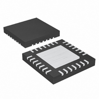
MAX17061ETI+ Maxim Integrated Products, MAX17061ETI+ Datasheet - Page 22

MAX17061ETI+
Manufacturer Part Number
MAX17061ETI+
Description
IC LED DRVR WHITE BCKLGT 28-TQFN
Manufacturer
Maxim Integrated Products
Type
Backlight, White LEDr
Datasheet
1.MAX17061ETI.pdf
(26 pages)
Specifications of MAX17061ETI+
Topology
PWM, Step-Up (Boost)
Number Of Outputs
8
Internal Driver
Yes
Type - Primary
Automotive, Backlight
Type - Secondary
White LED
Frequency
1MHz
Voltage - Supply
4.5 V ~ 26 V
Voltage - Output
5V
Mounting Type
Surface Mount
Package / Case
28-TQFN Exposed Pad
Operating Temperature
-40°C ~ 85°C
Current - Output / Channel
30mA
Internal Switch(s)
Yes
Operating Supply Voltage
5 V
Maximum Supply Current
2 mA
Maximum Power Dissipation
1667 mW
Maximum Operating Temperature
+ 85 C
Mounting Style
SMD/SMT
Minimum Operating Temperature
- 40 C
Lead Free Status / RoHS Status
Lead free / RoHS Compliant
Efficiency
-
Lead Free Status / Rohs Status
Lead free / RoHS Compliant
The peak-inductor current at minimum input voltage is
calculated as follows:
Alternatively, choosing a DCM operating mode at 750kHz
and estimating efficiency of 85% at this operating point:
A 4.7µH inductor is chosen. The peak inductor current
at minimum input voltage is calculated as follows:
The total output voltage ripple has two components: the
capacitive ripple caused by the charging and discharging
on the output capacitor, and the ohmic ripple due to the
capacitor’s equivalent series resistance (ESR):
and:
where I
Inductor Selection section).
The output voltage ripple should be low enough for the
FB_ current-source regulation. The ripple voltage should
be less than 200mV
put voltage ripple is typically dominated by V
The voltage rating and temperature characteristics of the
output capacitor must also be considered. The actual
capacitance of a ceramic capacitor is reduced by DC
voltage biasing. Ensure the selected capacitor has
enough capacitance at actual DC biasing.
8-String White LED Driver with
SMBus for LCD Panel Applications
22
I
PEAK
L
DCM MAX
V
______________________________________________________________________________________
RIPPLE C
I
PEAK
(
PEAK
4 7
V
100
.
RIPPLE
V
( )
)
uH
RIPPLE ESR
mA
is the peak inductor current (see the
2 10
100
2 0 825
1
0 675
I
7
OUT MAX
mA
.
V
2 35 9
7
35 9
C
P-P
(
.
Output Capacitor Selection
V
V
OUT
H
(
.
RIPPLE C
MHz
0 85
. For ceramic capacitors, the out-
.
35 9
V
)
MHz
.
7
35 9
(
35 9
7
V
V
.
V
)
I
.
0 4
PEAK ESR COUT
.
)
V
0 85
( )
.
2
V
V
.
V
35 9
V
OUT MAX
35 9
.
0 85
V
7
R
0 9
.
.
V
OUT MAX OSC
V
V
.
RIPPLE ESR
35 9
(
V
MHz
0 4
.
(
(
.
100
V
V
)
(
0 4
mA
)
V
7
.
0 92
f
IN MIN
)
V
.
V
)
(
RIPPLE(C)
A
5 6
1 47
.
)
.
H
A
.
The MAX17061’s high switching frequency demands a
high-speed rectifier. Schottky diodes are recommend-
ed for most applications because of their fast recovery
time and low forward voltage. The diode should be
rated to handle the output voltage and the peak switch
current. Make sure that the diode’s peak current rating
is at least I
section and that its breakdown voltage exceeds the
output voltage.
The OV protection circuit should ensure the circuit safe
operation; therefore, the controller should limit the out-
put voltage within the ratings of all MOSFET, diode, and
output capacitor components, while providing sufficient
output voltage for LED current regulation. The OV pin is
tied to the center tap of a resistive voltage-divider (R1
and R2 in Figure 1) from the high-voltage output. When
the controller detects the OV pin voltage reaching the
threshold V
vated. Hence, the step-up converter output overvoltage
protection point is:
In Figure 1, the output OVP voltage is set to:
The input capacitor (C
drawn from the input supply and reduces noise injec-
tion into the IC. A 10µF ceramic capacitor is used in the
Typical Operating Circuit (Figure 1) because of the
high source impedance seen in typical lab setups.
Actual applications usually have much lower source
impedance since the step-up regulator often runs
directly from the output of another regulated supply. In
some applications, C
ues used in the Typical Operating Circuit (Figure 1).
Ensure a low-noise supply at IN by using adequate C
Alternatively, greater voltage variation can be tolerated
on C
pass filter.
IN
Overvoltage Protection Determination
if IN is decoupled from C
V
OUT OVP
OV_TH
PEAK
V
(
OUT OVP
, typically 1.23V, OV protection is acti-
calculated in the Inductor Selection
)
(
1 236
IN
.
Input Capacitor Selection
)
Rectifier Diode Selection
can be reduced below the val-
IN
V
V
OV TH
) filters the current peaks
(
_
1
2 21
61 9
.
IN
.
1
M
using an RC low-
k
R
R
2
1
)
45
V
IN
.


