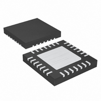
MAX17061ETI+ Maxim Integrated Products, MAX17061ETI+ Datasheet - Page 23

MAX17061ETI+
Manufacturer Part Number
MAX17061ETI+
Description
IC LED DRVR WHITE BCKLGT 28-TQFN
Manufacturer
Maxim Integrated Products
Type
Backlight, White LEDr
Datasheet
1.MAX17061ETI.pdf
(26 pages)
Specifications of MAX17061ETI+
Topology
PWM, Step-Up (Boost)
Number Of Outputs
8
Internal Driver
Yes
Type - Primary
Automotive, Backlight
Type - Secondary
White LED
Frequency
1MHz
Voltage - Supply
4.5 V ~ 26 V
Voltage - Output
5V
Mounting Type
Surface Mount
Package / Case
28-TQFN Exposed Pad
Operating Temperature
-40°C ~ 85°C
Current - Output / Channel
30mA
Internal Switch(s)
Yes
Operating Supply Voltage
5 V
Maximum Supply Current
2 mA
Maximum Power Dissipation
1667 mW
Maximum Operating Temperature
+ 85 C
Mounting Style
SMD/SMT
Minimum Operating Temperature
- 40 C
Lead Free Status / RoHS Status
Lead free / RoHS Compliant
Efficiency
-
Lead Free Status / Rohs Status
Lead free / RoHS Compliant
The series/parallel configuration of the LED load and the
full-scale bias current have a significant effect or regula-
tor performance. LED characteristics vary significantly
from manufacturer to manufacturer. Consult the respec-
tive LED data sheets to determine the range of output
voltages for a given brightness and LED current. In gen-
eral, brightness increases as a function of bias current.
This suggests that the number of LEDs could be
decreased if higher bias current is chosen; however,
high current increases LED temperature and reduces
operating life. Improvements in LED technology are
resulting in devices with lower forward voltage and
while increasing the bias current and light output.
LED manufacturers specify LED color at a given LED
current. With lower LED current, the color of the emitted
light tends to shift toward the blue range of the spec-
trum. A blue bias is often acceptable for business appli-
cations but not for high-image-quality applications such
as DVD players. Direct DPWM dimming is a viable solu-
tion for reducing power dissipation while maintaining
LED color integrity. Careful attention should be paid to
switching noise to avoid other display quality problems.
Using fewer LEDs in a string improves step-up converter
efficiency, and lowers breakdown voltage requirements
of the external MOSFET and diode. The minimum num-
ber of LEDs in series should always be greater than
maximum input voltage. If the diode voltage drop is
lower than maximum input voltage, the voltage drop
across the current-sense inputs (FB_) increases and
causes excess heating in the IC. Between 8 and 12
LEDs in series are ideal for input voltages up to 20V.
The MAX17061 has accurate (±1.5%) matching for
each current source. However, the forward voltage of
each white LED can vary up to 25% from part to part.
The accumulated voltage difference in each string
equates to additional power loss within the IC. For the
best efficiency, the voltage difference between strings
should be minimized. The difference between lowest
voltage string and highest voltage string should be less
than 4.8V (typ). Otherwise, the internal LED short-
protection circuit disables the high FB string.
Applications Information
______________________________________________________________________________________
LED Selection and Bias
LED V
SMBus for LCD Panel Applications
FB_
8-String White LED Driver with
Variation
The current through each FB_ pin is controlled only
during the step-up converter’s on-time. During the con-
verter’s off-time, the current sources are turned off. The
output voltage does not discharge and stays high. The
MAX17061 disables the FB current source to which the
string is shorted. In this case, the step-up converter’s
output voltage is always applied to the disabled FB pin.
The FB_ pin can withstand 45V.
Careful PCB layout is important for proper operation.
Use the following guidelines for good PCB layout:
1) Minimize the area of high current switching loop of
2) Connect high-current input and output components
3) Create a ground island (PGND) consisting of the
rectifier diode, internal MOSFET, and output capac-
itor to avoid excessive switching noise.
with short and wide connections. The high-current
input loop goes from the positive terminal of the input
capacitor to the inductor, to the internal MOSFET,
then to the input capacitor’s negative terminal. The
high-current output loop is from the positive termi-
nal of the input capacitor to the inductor, to the rec-
tifier diode, to the positive terminal of the output
capacitors, reconnecting between the output
capacitor and input capacitor ground terminals.
Avoid using vias in the high-current paths. If vias
are unavoidable, use multiple vias in parallel to
reduce resistance and inductance.
input and output capacitor ground and negative ter-
minal of the current-sense resistor. Connect all
these together with short, wide traces or a small
ground plane. Maximizing the width of the power-
ground traces improves efficiency and reduces out-
put-voltage ripple and noise spikes. Create an
analog ground island (AGND) consisting of the
overvoltage detection divider ground connection,
the ISET and FSET resistor connections, CCV
capacitor connections, and the device’s exposed
backside pad. Connect the AGND and PGND
islands by connecting the GND pins directly to the
exposed backside pad. Make no other connections
between these separate ground planes.
FB Pin Maximum Voltage
PCB Layout Guidelines
23


