LM3553SDX/NOPB National Semiconductor, LM3553SDX/NOPB Datasheet - Page 4
LM3553SDX/NOPB
Manufacturer Part Number
LM3553SDX/NOPB
Description
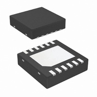
IC LED DRIVER PHOTO FLASH 12-LLP
Manufacturer
National Semiconductor
Series
PowerWise®r
Type
Photo Flash LED (I²C Interface)r
Datasheet
1.LM3553SDNOPB.pdf
(18 pages)
Specifications of LM3553SDX/NOPB
Topology
Step-Up (Boost)
Number Of Outputs
1
Internal Driver
Yes
Type - Primary
Backlight, Flash/Torch
Frequency
1MHz ~ 1.35MHz
Voltage - Supply
2.7 V ~ 5.5 V
Mounting Type
Surface Mount
Package / Case
12-LLP
Operating Temperature
-30°C ~ 85°C
Current - Output / Channel
1.2A
Internal Switch(s)
Yes
Efficiency
90%
For Use With
LM3553SDEV - BOARD EVALUATION FOR LM3553S
Lead Free Status / RoHS Status
Lead free / RoHS Compliant
Voltage - Output
-
Other names
LM3553SDX
Available stocks
Company
Part Number
Manufacturer
Quantity
Price
Company:

Part Number:
LM3553SDX/NOPB
Manufacturer:
NS
Quantity:
344


www.national.com
f
t
D
D
Th
Multi-Function Pin (M/F) Voltage Specifications
V
V
I
VIO
V
V
V
I
t
t
t
t
t
SW
FD-MIN
2
2
1
2
3
4
5
M/F
OL
C Compatible Voltage Specifications (SCL, SDIO, VIO)
IL
IH
OL
C Compatible Interface Timing Specifications (SCL, SDIO, VIO)
MAX
MIN
Symbol
Note 1: Absolute Maximum Ratings indicate limits beyond which damage to the component may occur. Operating Ratings are conditions under which operation
of the device is guaranteed. Operating Ratings do not imply guaranteed performance limits. For guaranteed performance limits and associated test conditions,
see the Electrical Characteristics tables.
Note 2: All voltages are with respect to the potential at the GND pin.
Note 3: Internal thermal shutdown circuitry protects the device from permanent damage. Thermal shutdown engages at T
T
Note 4: For detailed soldering specifications and information, please refer to National Semiconductor Application Note: AN-1187 for Recommended Soldering
Profiles.
Note 5: The human body model is a 100pF capacitor discharged through a 1.5kΩ resistor into each pin. (MIL-STD-883 3015.7)
Note 6: In applications where high power dissipation and/or poor package thermal resistance is present, the maximum ambient temperature may have to be
derated. Maximum ambient temperature (T
dissipation of the device in the application (P
following equation: T
Note 7: Junction-to-ambient thermal resistance is highly application and board-layout dependent. In applications where high maximum power dissipation exists,
special care must be paid to thermal dissipation issues in board design.
TX,F-EN
J
=120ºC (typ.).
Switching Frequency
Minimum Flash Duration Step t
Maximum Duty Cycle
Minimum Duty Cycle
TX, F
Multi-Function Pin Threshold
Voltages
Output Logic Low "0"
Serial Bus Voltage Level
Input Logic Low "0"
Input Logic High "1"
Output Logic Low "0"
SCL (Clock Period)
Data In Setup Time to SCL
High
Data Out stable After SCL Low
SDA Low Setup Time to SCL
Low (Start)
SDA High Hold Time After SCL
High (Stop)
EN
A-MAX
Pin Threshold
Parameter
= T
J-MAX-OP
– (θ
JA
A-MAX
× P
D-MAX
D-MAX
) is dependent on the maximum operating junction temperature (T
), and the junction-to-ambient thermal resistance of the part/package in the application (θ
On
Off
Input Logic High "1"
Input Logic Low "0"
I
GPIO Mode
VIO = 3.0V
VIO = 3.0V
I
).
FD-MIN
LOAD
LOAD
= 4.2mA,
= 3.7mA
= 16 ÷ f
Conditions
SW
4
0.55 × VIO
0.94
1.45
Min
100
100
100
1.0
1.0
2.5
0
0
0
0
J-MAX-OP
12.8
Typ
1.2
92
6
J
=140ºC (typ.) and disengages at
= 125ºC), the maximum power
20171411
0.38 ×VIO
Max
1.35
0.64
VIO
VIN
VIN
400
VIN
400
0.6
JA
), as given by the
Units
µsec.
MHz
mV
mV
µs
ns
ns
ns
ns
%
%
V
V
V
V
V
Related parts for LM3553SDX/NOPB
Image
Part Number
Description
Manufacturer
Datasheet
Request
R

Part Number:
Description:
LM3553 1.2A Dual Flash LED Driver System with I 2 C Compatible Interface; Package: LLP; No of Pins: 12; Qty per Container: 4500; Container: Reel
Manufacturer:
National Semiconductor
Datasheet:
Part Number:
Description:
1.2A Dual Flash LED Driver System with I2C Compatible
Manufacturer:
National Semiconductor
Datasheet:

Part Number:
Description:
1.2A Dual Flash LED Driver System with I2C Compatible
Manufacturer:
NSC [National Semiconductor]
Datasheet:

Part Number:
Description:
IC LED DRIVER PHOTO FLASH 12-LLP
Manufacturer:
National Semiconductor
Datasheet:
Part Number:
Description:
1.2A Dual Flash LED Driver System with I2C Compatible
Manufacturer:
National Semiconductor
Datasheet:
Part Number:
Description:
1.2A Dual Flash LED Driver System with I2C Compatible
Manufacturer:
National Semiconductor
Datasheet:
Part Number:
Description:
National Semiconductor [8-Bit D/A Converter]
Manufacturer:
National Semiconductor
Datasheet:
Part Number:
Description:
National Semiconductor [Media Coprocessor]
Manufacturer:
National Semiconductor
Datasheet:
Part Number:
Description:
Digitally Controlled Tone and Volume Circuit with Stereo Audio Power Amplifier, Microphone Preamp Stage and National 3D Sound
Manufacturer:
National Semiconductor
Datasheet:
Part Number:
Description:
Digitally Controlled Tone and Volume Circuit with Stereo Audio Power Amplifier, Microphone Preamp Stage and National 3D Sound
Manufacturer:
National Semiconductor
Datasheet:
Part Number:
Description:
AC97 Rev 2 Codec with Sample Rate Conversion and National 3D Sound
Manufacturer:
National Semiconductor
Part Number:
Description:
Manufacturer:
National Semiconductor
Datasheet:
Part Number:
Description:
Manufacturer:
National Semiconductor
Datasheet:
Part Number:
Description:
General Purpose, Low Voltage, Low Power, Rail-to-Rail Output Operational Amplifiers
Manufacturer:
National Semiconductor
Datasheet: