LM3553SDX/NOPB National Semiconductor, LM3553SDX/NOPB Datasheet - Page 8
LM3553SDX/NOPB
Manufacturer Part Number
LM3553SDX/NOPB
Description
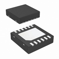
IC LED DRIVER PHOTO FLASH 12-LLP
Manufacturer
National Semiconductor
Series
PowerWise®r
Type
Photo Flash LED (I²C Interface)r
Datasheet
1.LM3553SDNOPB.pdf
(18 pages)
Specifications of LM3553SDX/NOPB
Topology
Step-Up (Boost)
Number Of Outputs
1
Internal Driver
Yes
Type - Primary
Backlight, Flash/Torch
Frequency
1MHz ~ 1.35MHz
Voltage - Supply
2.7 V ~ 5.5 V
Mounting Type
Surface Mount
Package / Case
12-LLP
Operating Temperature
-30°C ~ 85°C
Current - Output / Channel
1.2A
Internal Switch(s)
Yes
Efficiency
90%
For Use With
LM3553SDEV - BOARD EVALUATION FOR LM3553S
Lead Free Status / RoHS Status
Lead free / RoHS Compliant
Voltage - Output
-
Other names
LM3553SDX
Available stocks
Company
Part Number
Manufacturer
Quantity
Price
Company:

Part Number:
LM3553SDX/NOPB
Manufacturer:
NS
Quantity:
344


www.national.com
Block Diagram
Circuit Description
CIRCUIT COMPONENTS
F
The flash enable pin, F
I
'1', the flash current level defined through the I2C interface,
will be delived to the Flash LED. If the F
during the flash pulse, the flash event will stop. In the event
that F
will continue to deliver the flash current until the safety timer
duration (set through the I2C interface) is reached.
The LM3553 does not provide a fixed off-time after the flash
pulse has ended. Most flash LED manufacturers require that
the flash pulse duration be 10% of the total Flash cycle. Ex-
ample: If the flash pulse duration is set to be 200 milliseconds
(Flash Duration Code= 0011), the recommended off time for
the LED would be 1.8 seconds. Please consult the LED man-
ufacturers datasheet for exact timing requirements.
If the LM3553 is placed in indicator mode or torch mode
through the I
then low, at the end of the flash event, the LM3553 will return
to the mode stored in the General Purpose Register.
It is recommended that an external pull-down be placed be-
tween the F
during system start-up due to unknown control logic states.
2
EN
C) for starting the flash pulse. When F
Pin
EN
is not pulled low during the flash pulse, the LM3553
EN
2
C interface and the F
pin and GND to prevent unwanted LED flashing
EN
, provides an external method (non-
EN
pin is pulled high and
EN
EN
is pulled high, logic
pin is driven low
8
T
The transmission pin (T
drawn from the battery during a PA transmission. When the
T
LM3553 will switch to the programmed torch current level.
Once the T
to the flash current if this event occurs within the original flash
duration.
It is recommended that an external pull-down be placed be-
tween the T
during system start-up due to unknown control logic states.
M/F Pin
The multi-function pin (M/F) can be configured to provide
hardware RESET or a general purpose input/output (GPIO).
All functionality is programmed through the I
interface and set in the M/F pin functionality control register
(address 0x20). The default function is a RESET, where a
logic '1' places the part in the normal operating mode, and a
logic '0' places the part into a RESET state. A reset condition
will place all LM3553 registers into their default states.
X
X
Pin
pin is driven high (logic '1') during a flash pulse, the
X
X
pin is driven low (logic '0'), the LM3553 will return
pin and GND to prevent unwanted LED flashing
X
) can be used to limit the current
20171417
2
C compatible
Related parts for LM3553SDX/NOPB
Image
Part Number
Description
Manufacturer
Datasheet
Request
R

Part Number:
Description:
LM3553 1.2A Dual Flash LED Driver System with I 2 C Compatible Interface; Package: LLP; No of Pins: 12; Qty per Container: 4500; Container: Reel
Manufacturer:
National Semiconductor
Datasheet:
Part Number:
Description:
1.2A Dual Flash LED Driver System with I2C Compatible
Manufacturer:
National Semiconductor
Datasheet:

Part Number:
Description:
1.2A Dual Flash LED Driver System with I2C Compatible
Manufacturer:
NSC [National Semiconductor]
Datasheet:

Part Number:
Description:
IC LED DRIVER PHOTO FLASH 12-LLP
Manufacturer:
National Semiconductor
Datasheet:
Part Number:
Description:
1.2A Dual Flash LED Driver System with I2C Compatible
Manufacturer:
National Semiconductor
Datasheet:
Part Number:
Description:
1.2A Dual Flash LED Driver System with I2C Compatible
Manufacturer:
National Semiconductor
Datasheet:
Part Number:
Description:
National Semiconductor [8-Bit D/A Converter]
Manufacturer:
National Semiconductor
Datasheet:
Part Number:
Description:
National Semiconductor [Media Coprocessor]
Manufacturer:
National Semiconductor
Datasheet:
Part Number:
Description:
Digitally Controlled Tone and Volume Circuit with Stereo Audio Power Amplifier, Microphone Preamp Stage and National 3D Sound
Manufacturer:
National Semiconductor
Datasheet:
Part Number:
Description:
Digitally Controlled Tone and Volume Circuit with Stereo Audio Power Amplifier, Microphone Preamp Stage and National 3D Sound
Manufacturer:
National Semiconductor
Datasheet:
Part Number:
Description:
AC97 Rev 2 Codec with Sample Rate Conversion and National 3D Sound
Manufacturer:
National Semiconductor
Part Number:
Description:
Manufacturer:
National Semiconductor
Datasheet:
Part Number:
Description:
Manufacturer:
National Semiconductor
Datasheet:
Part Number:
Description:
General Purpose, Low Voltage, Low Power, Rail-to-Rail Output Operational Amplifiers
Manufacturer:
National Semiconductor
Datasheet: