CAT3636HV3-GT2 ON Semiconductor, CAT3636HV3-GT2 Datasheet - Page 7
CAT3636HV3-GT2
Manufacturer Part Number
CAT3636HV3-GT2
Description
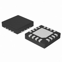
IC LED DVR 6CH QUAD MODE 16TQFN
Manufacturer
ON Semiconductor
Series
QUAD-Mode®r
Type
Backlight, White LEDr
Datasheet
1.CAT3636HV3-T2.pdf
(14 pages)
Specifications of CAT3636HV3-GT2
Topology
Linear (LDO), Switched Capacitor (Charge Pump)
Number Of Outputs
6
Internal Driver
Yes
Type - Primary
Backlight
Type - Secondary
RGB, White LED
Frequency
600kHz ~ 1.4MHz
Voltage - Supply
2.5 V ~ 5.5 V
Voltage - Output
7V
Mounting Type
Surface Mount
Package / Case
16-TFQFN Exposed Pad
Operating Temperature
-40°C ~ 85°C
Current - Output / Channel
32mA
Internal Switch(s)
Yes
Efficiency
92%
Lead Free Status / RoHS Status
Lead free / RoHS Compliant
Available stocks
Company
Part Number
Manufacturer
Quantity
Price
Company:

Part Number:
CAT3636HV3-GT2
Manufacturer:
ON Semiconductor
Quantity:
57 653
Company:
Part Number:
CAT3636HV3-GT2
Manufacturer:
ON Semiconductor
Quantity:
950


Pin Function
VIN is the supply pin for the charge pump. A small 1 mF
ceramic bypass capacitor is required between the VIN pin
and ground near the device. The operating input voltage
range is from 2.5 V to 5.5 V. Whenever the input supply falls
below the under−voltage threshold (2 V) all the LED
channels will be automatically disabled and the device
register are reset to default values.
EN/SET is the enable and one wire addressable control logic
input for all LED channels. Guaranteed levels of logic high
and logic low are set at 1.3 V and 0.4 V respectively. When
EN/SET is initially taken high, the device becomes enabled
and all LED currents remain at 0 mA. To place the device
into zero current mode, the EN/SET pin must be held low for
more than 1.5 ms.
VOUT is the charge pump output that is connected to the
LED anodes. A small 1 mF ceramic bypass capacitor is
required between the VOUT pin and ground near the device.
Table 5. PIN DESCRIPTION
13/14
Pin #
TAB
10
11
12
15
16
1
2
3
4
5
6
7
8
9
EN/SET
LEDC2
LEDC1
LEDB2
LEDB1
LEDA2
LEDA1
VOUT
Name
GND
C1+
C2+
TAB
C1−
C2−
VIN
NC
LEDC2 cathode terminal
LEDC1 cathode terminal
LEDB2 cathode terminal
LEDB1 cathode terminal
LEDA2 cathode terminal
LEDA1 cathode terminal
Charge pump output, connect to LED anodes
Charge pump input, connect to battery or supply
Bucket capacitor 1, positive terminal
Bucket capacitor 1, negative terminal
Bucket capacitor 2, positive terminal
Bucket capacitor 2, negative terminal
No connect
Ground reference
Device enable (active high) and 1 wire control input
Connect to GND on the PCB
http://onsemi.com
7
GND is the ground reference for the charge pump. The pin
must be connected to the ground plane on the PCB.
C1+, C1− are connected to each side of the ceramic bucket
capacitor C1.
C2+, C2− are connected to each side of the ceramic bucket
capacitor C2.
LEDxx provide the internal regulated current for each of the
LED cathodes. These pins enter high−impedance zero
current state whenever the device is placed in shutdown
mode.
TAB is the exposed pad underneath the package. For best
thermal performance, the tab should be soldered to the PCB
and connected to the ground plane.
Function
Related parts for CAT3636HV3-GT2
Image
Part Number
Description
Manufacturer
Datasheet
Request
R

Part Number:
Description:
ON Semiconductor [VOLTAGE REGULATOR]
Manufacturer:
ON Semiconductor
Datasheet:
Part Number:
Description:
357-036-542-201 CARDEDGE 36POS DL .156 BLK LOPRO
Manufacturer:
ON Semiconductor
Datasheet:
Part Number:
Description:
357-036-542-201 CARDEDGE 36POS DL .156 BLK LOPRO
Manufacturer:
ON Semiconductor
Datasheet:
Part Number:
Description:
357-036-542-201 CARDEDGE 36POS DL .156 BLK LOPRO
Manufacturer:
ON Semiconductor
Datasheet:
Part Number:
Description:
357-036-542-201 CARDEDGE 36POS DL .156 BLK LOPRO
Manufacturer:
ON Semiconductor
Datasheet:
Part Number:
Description:
357-036-542-201 CARDEDGE 36POS DL .156 BLK LOPRO
Manufacturer:
ON Semiconductor
Datasheet:
Part Number:
Description:
357-036-542-201 CARDEDGE 36POS DL .156 BLK LOPRO
Manufacturer:
ON Semiconductor
Datasheet:
Part Number:
Description:
357-036-542-201 CARDEDGE 36POS DL .156 BLK LOPRO
Manufacturer:
ON Semiconductor
Datasheet:
Part Number:
Description:
357-036-542-201 CARDEDGE 36POS DL .156 BLK LOPRO
Manufacturer:
ON Semiconductor
Datasheet:
Part Number:
Description:
357-036-542-201 CARDEDGE 36POS DL .156 BLK LOPRO
Manufacturer:
ON Semiconductor
Datasheet:
Part Number:
Description:
357-036-542-201 CARDEDGE 36POS DL .156 BLK LOPRO
Manufacturer:
ON Semiconductor
Datasheet:
Part Number:
Description:
Manufacturer:
ON Semiconductor
Datasheet:
Part Number:
Description:
Manufacturer:
ON Semiconductor
Datasheet:
Part Number:
Description:
Manufacturer:
ON Semiconductor
Datasheet: