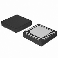
CAT9552HV6I-GT2 ON Semiconductor, CAT9552HV6I-GT2 Datasheet

CAT9552HV6I-GT2
Specifications of CAT9552HV6I-GT2
Related parts for CAT9552HV6I-GT2
CAT9552HV6I-GT2 Summary of contents
Page 1
I C-bus LED Driver with Programmable Blink Rate FEATURES 16 LED drivers with On/Off and programmable blink rate control 2 selectable, programmable blink rates: – frequency: 0.172Hz to 44Hz – duty cycle 99.6% 16 open drain ...
Page 2
CAT9552 PIN CONFIGURATION SOIC (W), TSSOP ( SDA SCL LED0 4 21 RESET LED1 5 20 LED15 LED2 6 19 LED14 LED3 7 19 LED13 LED4 8 17 LED12 ...
Page 3
ABSOLUTE MAXIMUM RATINGS Parameters V with Respect to Ground CC Voltage on Any Pin with Respect to Ground DC Current on I/Os Supply Current Package Power Dissipation Capability (T Junction Temperature Storage Temperature Lead Soldering Temperature (10 seconds) Operating Ambient ...
Page 4
CAT9552 D.C. OPERATING CHARACTERISTICS V = 2.3 to 5.5V 0V -40ºC to +85ºC, unless otherwise specified Symbol Parameter Supplies V Supply Voltage CC I Supply Current CC I Standby Current stb Δ I ...
Page 5
A.C. CHARACTERISTICS V = 2.3V to 5.5V -40ºC to +85ºC, unless otherwise specified CC A Symbol Parameter F Clock Frequency SCL t START Condition Hold Time HD:STA t Low Period of SCL Clock LOW t High Period of ...
Page 6
CAT9552 AC TEST CONDITIONS Input Pulse Voltage Input Rise and Fall Times Input Reference Voltage Output Reference Voltage Output Load t F SCL t SU:STA SDA IN SDA OUT PIN DESCRIPTION SCL: Serial Clock The serial clock input clocks all ...
Page 7
FUNCTIONAL DESCRIPTION The CAT9552 is a 16-channel I/O bus expander that provides a pair of programmable LED blinkers, 2 controlled through compatible serial interface. 2 CAT9552 supports the I C Bus data transmission protocol. This Inter-Integrated Circuit ...
Page 8
CAT9552 Acknowledge After a successful data transfer, each receiving device is required to generate an acknowledge. The acknowledging device pulls down the SDA line during the ninth clock cycle, signaling that it received the 8 bits of data. The SDA ...
Page 9
Input Register 0 and Input Register 1 reflect the incoming logic levels of the I/O pins, regardless of whether the pin is defined as an input or an output. These registers are read only ports. Writes to the input registers ...
Page 10
CAT9552 Write Operations Data is transmitted to the CAT9552 registers using the write sequence shown in Figure 6. If the AI bit from the command byte is set to “1”, the CAT9552 internal registers can be written sequentially. After sending ...
Page 11
External Reset Operation 2 The CAT9552 registers and the I C state machine are initialized to their default state when the RESET input is held low for a minimum CAT9552’s registers W will be held in their ...
Page 12
CAT9552 APPLICATION INFORMATION Programming Example The following programming sequence is an example how to set: – LED0 to LED3: ON – LED4 to LED7: Blink at 1Hz with a 50% duty cycle (Blink 0) – LED8 to LED11: Blink at ...
Page 13
PACKAGE OUTLINE DRAWINGS (1)(2) SOIC 24-Lead ( PIN#1 IDENTIFICATION TOP VIEW D A SIDE VIEW Notes: (1) All dimensions are in millimeters. Angles in degrees. (2) Complies with JEDEC MS-013. © 2010 SCILLC. All rights reserved Characteristics subject ...
Page 14
CAT9552 (1)(2) TSSOP 24-Lead 4.4mm (Y) e TOP VIEW SIDE VIEW Notes: (1) All dimensions are in millimeters. Angles in degrees. (2) Complies with JEDEC MO-153. Doc. No. MD-9005 Rev θ1 14 ...
Page 15
TQFN 24-Pad 4 x 4mm (HV6) D PIN#1 INDEX AREA SYMBOL MIN NOM A 0.70 0.75 A1 0.00 A3 0.20 REF b 0.20 0.25 D 4.00 BSC D2 2.70 2.80 E 4.00 ...
Page 16
CAT9552 (1)(2)(3) TQFN 24-PAD 4 X 4MM (HT6) D PIN#1 INDEX AREA SYMBOL MIN NOM A 0.70 0.75 A1 0.00 — A3 0.20 REF b 0.20 0.25 D 4.00 BSC D2 2.00 — ...
Page 17
... The standard plated finish is Matte-Tin for SOIC and TSSOP packages. The standard plated finish is NiPdAu for TQFN package. (3) The device used in the above example is a CAT9552HV6I-GT2 (TQFN, Industrial Temperature, NiPdAu, Tape & Reel, 2,000/Reel). (4) For additional temperature options, please contact your nearest ON Semiconductor Sales office. ...
Page 18
... Date Description 23-Jun-08 A Initial Issue Update A.C. Characteristics table to include Standard I 03-Dec-08 B Change logo and fine print to ON Semiconductor 09-Jul-09 C Update Table 5. LED Selector Registers 22-Jan-10 D Update TQFN Packages ON Semiconductor and are registered trademarks of Semiconductor Components Industries, LLC (SCILLC). SCILLC reserves the right to make changes without further notice to any products herein ...


