CAT9552HV6I-GT2 ON Semiconductor, CAT9552HV6I-GT2 Datasheet - Page 10
CAT9552HV6I-GT2
Manufacturer Part Number
CAT9552HV6I-GT2
Description
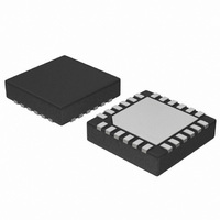
IC LED DRIVER LINEAR 24-TQFN
Manufacturer
ON Semiconductor
Type
Linear (I²C Interface)r
Datasheet
1.CAT9552YI-T2.pdf
(18 pages)
Specifications of CAT9552HV6I-GT2
Topology
PWM
Number Of Outputs
16
Internal Driver
Yes
Type - Primary
LED Blinker
Frequency
400Hz
Voltage - Supply
2.3 V ~ 5.5 V
Mounting Type
Surface Mount
Package / Case
24-TFQFN Exposed Pad
Operating Temperature
-40°C ~ 85°C
Current - Output / Channel
25mA
Internal Switch(s)
Yes
Number Of Segments
16
Low Level Output Current
25 mA
Operating Supply Voltage
2.3 V to 5.5 V
Maximum Supply Current
550 uA
Maximum Power Dissipation
1 W
Maximum Operating Temperature
+ 85 C
Mounting Style
SMD/SMT
Minimum Operating Temperature
- 40 C
Lead Free Status / RoHS Status
Lead free / RoHS Compliant
Voltage - Output
-
Efficiency
-
Lead Free Status / Rohs Status
Details


FROM PORT
REGISTER
CAT9552
Write Operations
Data is transmitted to the CAT9552 registers using the
write sequence shown in Figure 6.
If the AI bit from the command byte is set to “1”, the
CAT9552 internal registers can be written sequentially.
After sending data to one register, the next data byte
will be sent to the next register sequentially
addressed.
Read Operations
The CAT9552 registers are read according to the
timing diagrams shown in Figure 7 and Figure 8. Data
from the register, defined by the command byte, will
be sent serially on the SDA line.
After the first byte is read, additional data bytes may
be read when the auto-increment flag, AI, is set. The
additional data byte will reflect the data read from the
next register sequentially addressed by the (B3, B2,
B1, B0) bits of the command byte.
When reading Input Port Registers (Figure 8), data is
clocked into the register on the failing edge of the
acknowledge clock pulse. The transfer is stopped
when the master will not acknowledge the data byte
received and issue the STOP condition.
WRITE TO
DATA OUT
Doc. No. MD-9005 Rev D
SCL
SDA
Note: Transfer can be stopped at any time by a STOP condition.
S
1
Start Condition
S
1
1
1
Slave Address
0
2
1
Slave Address
0
3
0
A2 A1 A0
4
0
A2 A1 A0
5
6
Acknowledge
R/W
From Slave
0
7
R/W Acknowledge
A
8
0
Figure 7. Read from Register Timing Diagram
A
9
From Slave
Figure 6. Write to Register Timing Diagram
0
COMMAND BYTE
0
0
Command Byte
AI
B3 B2 B1 B0
Acknowledge
From Slave
At This Moment Master-Transmitter
A
Becomes Master-receiver and
10
S
A
Acknowledge
From Slave
Slave-Receiver Becomes
LED Pins Used as General Purpose I/O
Any LED pins not used to drive LEDs can be used as
general purpose input/output, GPIO.
When used as input, the user should program the
corresponding LED pin to Hi-Z (“01” for the LSx
register bits). The pin state can be read via the
Input Register according to the sequence shown in
Figure 8.
For use as a logic output, an external pull-up resistor
should be connected to the pin. The value of the pull-
up resistor is calculated according to the DC operating
characteristics. To set the output high, the user has to
program the output Hi-Z writing “01” into the
corresponding LED Selector (LSx) register bits. The
output pin is set low when the output is programmed
low through the LSx register bits (“00” in LSx register
bits).
GPIO can also be used as PWM outputs by setting the
LED Selector (LSx) register to “10” or “11” to output
either
1
1
Slave-Transmitter
Slave Address
Data To Register 1
0
DAT
0
the
A
A2 A1 A0
1
BLINK0
Acknowledge
From Slave
R/W
t
pv
1
MSB
A
A
Acknowledge
From Slave
Data From Register
MSB
Characteristics subject to change without notice
or
Last Byte
Data From Register
Data To Register 2
DATA
Register Address
First Byte
Auto-increment
BLINK1
DATA
© 2010 SCILLC. All rights reserved
If Al = 1
LSB
No Acknowledge
From Master
NA
Acknowledge
From Master
LSB
1.0
waveform.
P
A
A
Related parts for CAT9552HV6I-GT2
Image
Part Number
Description
Manufacturer
Datasheet
Request
R

Part Number:
Description:
ON Semiconductor [VOLTAGE REGULATOR]
Manufacturer:
ON Semiconductor
Datasheet:
Part Number:
Description:
357-036-542-201 CARDEDGE 36POS DL .156 BLK LOPRO
Manufacturer:
ON Semiconductor
Datasheet:
Part Number:
Description:
357-036-542-201 CARDEDGE 36POS DL .156 BLK LOPRO
Manufacturer:
ON Semiconductor
Datasheet:
Part Number:
Description:
357-036-542-201 CARDEDGE 36POS DL .156 BLK LOPRO
Manufacturer:
ON Semiconductor
Datasheet:
Part Number:
Description:
357-036-542-201 CARDEDGE 36POS DL .156 BLK LOPRO
Manufacturer:
ON Semiconductor
Datasheet:
Part Number:
Description:
357-036-542-201 CARDEDGE 36POS DL .156 BLK LOPRO
Manufacturer:
ON Semiconductor
Datasheet:
Part Number:
Description:
357-036-542-201 CARDEDGE 36POS DL .156 BLK LOPRO
Manufacturer:
ON Semiconductor
Datasheet:
Part Number:
Description:
357-036-542-201 CARDEDGE 36POS DL .156 BLK LOPRO
Manufacturer:
ON Semiconductor
Datasheet:
Part Number:
Description:
357-036-542-201 CARDEDGE 36POS DL .156 BLK LOPRO
Manufacturer:
ON Semiconductor
Datasheet:
Part Number:
Description:
357-036-542-201 CARDEDGE 36POS DL .156 BLK LOPRO
Manufacturer:
ON Semiconductor
Datasheet:
Part Number:
Description:
357-036-542-201 CARDEDGE 36POS DL .156 BLK LOPRO
Manufacturer:
ON Semiconductor
Datasheet:
Part Number:
Description:
Manufacturer:
ON Semiconductor
Datasheet:
Part Number:
Description:
Manufacturer:
ON Semiconductor
Datasheet:
Part Number:
Description:
Manufacturer:
ON Semiconductor
Datasheet: