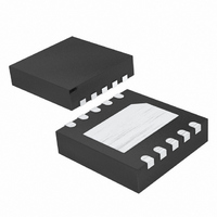
MAX1583ZETB+T Maxim Integrated Products, MAX1583ZETB+T Datasheet - Page 9

MAX1583ZETB+T
Manufacturer Part Number
MAX1583ZETB+T
Description
IC LED DRIVR PHOTO FLASH 10-TDFN
Manufacturer
Maxim Integrated Products
Type
Photo Flash LEDr
Datasheet
1.MAX1583XETBT.pdf
(10 pages)
Specifications of MAX1583ZETB+T
Constant Current
Yes
Topology
Step-Up (Boost)
Number Of Outputs
1
Internal Driver
Yes
Type - Primary
Flash/Torch
Type - Secondary
White LED
Frequency
750kHz ~ 1.25MHz
Voltage - Supply
2.6 V ~ 5.5 V
Voltage - Output
24V
Mounting Type
Surface Mount
Package / Case
10-TDFN Exposed Pad
Operating Temperature
-40°C ~ 85°C
Current - Output / Channel
250mA
Internal Switch(s)
Yes
Efficiency
80%
Number Of Segments
5
Operating Supply Voltage
2.6 V to 5.5 V
Maximum Power Dissipation
1951 mW
Maximum Operating Temperature
+ 85 C
Mounting Style
SMD/SMT
Minimum Operating Temperature
- 40 C
Lead Free Status / RoHS Status
Lead free / RoHS Compliant
Bypass the input to GND using a ceramic capacitor.
Place the capacitor as close to the IC as possible. The
exact value of the input capacitor is not critical. The
typical value for the input capacitor is 22µF when using
the MAX1583X, 10µF when using the MAX1583Y, and
4µF when using the MAX1583Z. Using these values
reduces the input ripple to an acceptable level.
The output capacitance required depends on the
required LED current and the time duration of the pulse
in strobe mode. See the Reservoir Capacitance vs.
Current Limit section for details on determining this
capacitance value. Note that the output capacitor must
be rated for 25V or greater. In addition to the reservoir
capacitor, bypass the output with a 0.1µF, 25V capaci-
tor from OUT to LED.
The recommended inductor values for use with the
MAX1583 range from 4.7µH to 47µH. With input volt-
ages near 5V, a larger value of inductance can be
more efficient. To prevent core saturation, ensure that
the inductor-saturation current rating exceeds the cur-
rent limit of the MAX1583 (250mA, 500mA, or 1A).
The MAX1583 requires a high-speed rectification diode
(D1) for optimum performance. A Schottky diode is rec-
ommended due to its fast recovery time and low for-
ward-voltage drop. Ensure that the diode’s average
and peak current ratings exceed the average output
current and the current limit (I
(250mA, 500mA, or 1A). In addition, the diode’s reverse
breakdown voltage must exceed V
current is calculated as:
I
DIODE RMS
(
_______________________________________________________________________________________
Output-Capacitor Selection
)
Input-Capacitor Selection
Schottky-Diode Selection
≅
I
LED MAX
(
Inductor Selection
LIMIT
OUT
)
×
) of the MAX1583
I
. The RMS diode
LIMIT
White LED Camera-Flash
Due to fast-switching waveforms and high-current
paths, careful PC board layout is required. An evalua-
tion kit (MAX1583EVKIT) is available as an example to
speed design. When laying out a board, minimize trace
lengths between the IC and the inductor, the diode, the
input capacitor, and the output capacitor. Keep traces
short, direct, and wide. The IN bypass capacitor should
be placed as close to the IC as possible. GND should
be connected directly to the exposed paddle under-
neath the IC. The ground connections of C
should be as close together as possible. The traces
from IN to the inductor and from the Schottky diode to
the LEDs can be longer.
TRANSISTOR COUNT: 1395
PROCESS: BiCMOS
+Denotes lead-free package.
MAX1583YETB-T
MAX1583YETB+T
MAX1583ZETB-T
MAX1583ZETB+T
PART
Applications Information
Boost Converter
-40°C to +85°C
-40°C to +85°C
-40°C to +85°C
-40°C to +85°C
TEMP RANGE
Ordering Information
Chip Information
PC Board Layout
PIN-PACKAGE
10 TDFN 3mm x 3mm
10 TDFN 3mm x 3mm
10 TDFN 3mm x 3mm
10 TDFN 3mm x 3mm
IN
and C
OUT
9


