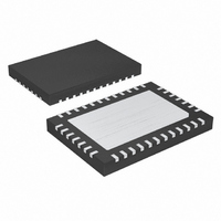
MAX16810ATU+T Maxim Integrated Products, MAX16810ATU+T Datasheet - Page 15

MAX16810ATU+T
Manufacturer Part Number
MAX16810ATU+T
Description
IC LED DRVR WT/RGB BCKLT 38-TQFN
Manufacturer
Maxim Integrated Products
Type
Backlight, White LED, RGB (Serial Interface)r
Specifications of MAX16810ATU+T
Constant Current
Yes
Topology
*
Number Of Outputs
16
Internal Driver
Yes
Type - Primary
Backlight
Type - Secondary
RGB, White LED
Frequency
20kHz ~ 1MHz
Voltage - Supply
8 V ~ 26.5 V
Voltage - Output
36V
Mounting Type
Surface Mount
Package / Case
38-TQFN Exposed Pad
Operating Temperature
-40°C ~ 125°C
Current - Output / Channel
55mA
Internal Switch(s)
No
Low Level Output Current
6 mA
High Level Output Current
1.8 mA
Operating Supply Voltage
3 V to 5.5 V
Maximum Supply Current
5 mA
Maximum Power Dissipation
2857 mW
Maximum Operating Temperature
+ 125 C
Mounting Style
SMD/SMT
Minimum Operating Temperature
- 40 C
Lead Free Status / RoHS Status
Lead free / RoHS Compliant
Efficiency
-
Lead Free Status / Rohs Status
Details
Table 1. 4-Wire Serial-Interface Truth Table
The MAX16809 also operates in a stand-alone mode
(see the Typical Operating Circuits ). For use with a
microcontroller, the MAX16809 features a 4-wire serial
interface using DIN, CLK, LE, OE inputs and DOUT as
a data output. This interface is used to write the LED
channels’ data to the MAX16809. The serial-interface
data word length is 16 bits, D0–D15. See Figure 3.
The functions of the five interface pins are as follows:
DIN is the serial-data input, and must be stable when it
is sampled on the rising edge of CLK. Data is shifted in
MSB first. This means that data bit D15 is clocked in
first, followed by 15 more data bits, finishing with the
LSB, D0.
CLK is the serial-clock input that shifts data at DIN into
the MAX16809’s 16-bit shift register on its rising edge.
L = Low Logic Level
H = High Logic Level
X = Don’t Care
P = Present State (Shift Register)
R = Previous State (Latched)
SERIAL
INPUT
DATA
DIN
H
L
X
CLOCK
INPUT
CLK
SHIFT REGISTER CONTENTS
D0 D1 D2 … Dn-1
R0 R1 R2 … Rn-1
P0
Switch-Mode Boost and SEPIC Controller
H
X
L
______________________________________________________________________________________
R0 R1 … Rn-2 Rn-1
R0 R1 … Rn-2 Rn-1
P1 P2 … Pn-1
X
Integrated 16-Channel LED Driver with
X
…
X
4-Wire Interface
LED Driver
Dn
Rn
Pn
X
INPUT
LOAD
LE
H
L
D0 D1 D2 … Dn-1 Dn
R0 R1 R2
P0 P1 P2
X
LATCH CONTENTS
X
LE is the latch-enable input of the MAX16809 that trans-
fers data from the 16-bit shift register to its 16-bit output
latches (transparent latch). The data latches on the
falling edge of LE (Figure 4). The fourth input (OE) pro-
vides output-enable control of the output drivers. When
OE is driven high, the outputs (OUT0–OUT15) are forced
to high impedance without altering the contents of the
output latches. Driving OE low enables the outputs to fol-
low the state of the output latches. OE is independent of
the serial interface operation. Data can be shifted into
the serial-interface shift register and latched, regardless
of the state of OE. DOUT is the serial-data output that
shifts data out from the MAX16809’s 16-bit shift register
on the rising edge of CLK. Data at DIN propagates
through the shift register and appears at DOUT 16 clock
cycles later. Table 1 shows the 4-wire serial-interface
truth table.
X
… Rn-1 Rn
… Pn-1 Pn
…
X
X
BLANKING
INPUT
OE
H
L
D0 D1 D2 …
P0 P1 P2
L
CURRENT AT OUT_ _
OUTPUT CONTENTS
L
L
…
…
Dn-1 Dn
Pn-1 Pn
L
15
L


