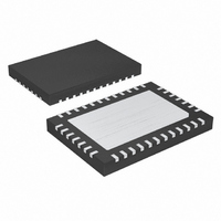
MAX16810ATU+T Maxim Integrated Products, MAX16810ATU+T Datasheet - Page 17

MAX16810ATU+T
Manufacturer Part Number
MAX16810ATU+T
Description
IC LED DRVR WT/RGB BCKLT 38-TQFN
Manufacturer
Maxim Integrated Products
Type
Backlight, White LED, RGB (Serial Interface)r
Specifications of MAX16810ATU+T
Constant Current
Yes
Topology
*
Number Of Outputs
16
Internal Driver
Yes
Type - Primary
Backlight
Type - Secondary
RGB, White LED
Frequency
20kHz ~ 1MHz
Voltage - Supply
8 V ~ 26.5 V
Voltage - Output
36V
Mounting Type
Surface Mount
Package / Case
38-TQFN Exposed Pad
Operating Temperature
-40°C ~ 125°C
Current - Output / Channel
55mA
Internal Switch(s)
No
Low Level Output Current
6 mA
High Level Output Current
1.8 mA
Operating Supply Voltage
3 V to 5.5 V
Maximum Supply Current
5 mA
Maximum Power Dissipation
2857 mW
Maximum Operating Temperature
+ 125 C
Mounting Style
SMD/SMT
Minimum Operating Temperature
- 40 C
Lead Free Status / RoHS Status
Lead free / RoHS Compliant
Efficiency
-
Lead Free Status / Rohs Status
Details
In stand-alone operation, the MAX16809 does not use
the 4-wire interface (see the Typical Operating
Circuits ). Connect DIN and LE to V+ and provide at
least 16 external clock pulses to CLK to enable 16 out-
put ports. This startup pulse sequence can be provided
either using an external clock or the PWM signal. The
external clock can also be generated using the signal
at RTCT and an external comparator.
All the output channels can be dimmed simultaneously
by applying a PWM signal (50Hz to 30kHz) to OE. This
allows for a wide range of dimming up to a 5000:1 ratio.
Each channel can be independently turned on and off
using a 4-wire serial interface. The dimming is propor-
tional to the PWM duty cycle.
Using an analog or digital potentiometer as R
for LED current amplitude adjustment and linear dimming.
Use the following equation to estimate the upper limit
power dissipation (PD) for the MAX16809:
PD DUTY
=
+
LED Current Amplitude Adjustment
(
V
CC
x I
×
Switch-Mode Boost and SEPIC Controller
Computing Power Dissipation
CC
______________________________________________________________________________________
⎡
⎢
⎢
⎣
(
V x I
)
+
Integrated 16-Channel LED Driver with
Stand-Alone Operation
+ + ∑
)
i
i
=
=
15
0
LED Dimming
V
OUTi
PWM Dimming
x
I
OUTi
SET
⎤
⎥
⎥
⎦
allows
where:
V+ = supply voltage
I+ = V+ operating supply current
DUTY = PWM duty cycle applied to OE
V
load LED(s)
I
PD = power dissipation
Careful PCB layout is critical to achieve low switching
losses and clean, stable operation. Use a multilayer
board whenever possible for better noise immunity.
Protect sensitive analog grounds by using a star
ground configuration. Minimize ground noise by con-
necting AGND, PGND, the input bypass-capacitor
ground lead, and the output-filter ground lead to a sin-
gle point (star ground configuration). Also, minimize
trace lengths to reduce stray capacitance, trace resis-
tance, and radiated noise. The trace between the out-
put voltage-divider and the FB pin must be kept short,
as well as the trace between AGND and PGND.
OUTi
OUTi
= LED drive current programmed by R
= MAX16809 port output voltage when driving
PCB Layout Guidelines
SET
17


