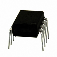
IRS2530DPBF International Rectifier, IRS2530DPBF Datasheet - Page 12

IRS2530DPBF
Manufacturer Part Number
IRS2530DPBF
Description
IC CTRL BALLAST DIMMING 8-DIP
Manufacturer
International Rectifier
Series
DIM8™r
Type
Ballast Controllerr
Datasheet
1.IRS2530DSTRPBF.pdf
(23 pages)
Specifications of IRS2530DPBF
Frequency
34.2 ~ 115 kHz
Current - Supply
5mA
Current - Output
260mA
Voltage - Supply
12.5 V ~ 15.6 V
Operating Temperature
-40°C ~ 125°C
Package / Case
8-DIP (0.300", 7.62mm)
Rohs Compliant
Yes
Peak Reflow Compatible (260 C)
Yes
Supply Current
5mA
Driver Case Style
DIP
No. Of Pins
8
Operating Temperature Range
-40°C To +125°C
Leaded Process Compatible
Yes
For Use With
IRPLDIM5E - KIT DES BALLAST 4LEVEL DIM FLUORIRPLDIM4E - KIT DES BALLAST 26W IRS2530DIRPLCFL8U - KIT DES FLUOR BALLAST IRS2530D
Lead Free Status / RoHS Status
Lead free / RoHS Compliant
Available stocks
Company
Part Number
Manufacturer
Quantity
Price
Company:
Part Number:
IRS2530DPBF
Manufacturer:
IR
Quantity:
3 825
Part Number:
IRS2530DPBF
Manufacturer:
IR
Quantity:
20 000
www.irf.com
Application Information and Additional Details
Information regarding the following topics is included as subsections within this section of the datasheet:
UVLO Mode and IC Supply Circuitry
The Under-Voltage Lock-Out Mode (UVLO) is defined as the state the IC is in when V
threshold of the IC, V
The UVLO circuit is designed to maintain an ultra-low supply current I
the IC is fully functional before the high- and low-side output gate drivers are activated. The VCC capacitor,
CVCC, is charged up from the DC bus voltage through supply resistors RVCC1 and RVCC2 (Figure 1). The
values of these resistors are chosen such that VCC reaches the UVLO+ turn-on threshold voltage at the
desired DC bus voltage level. Once the capacitor voltage on VCC reaches the start-up threshold, V
IC turns on and the HO and LO gate drive outputs start oscillating. The capacitor CVCC should be large
enough to hold the voltage at VCC above the V
and supply the required voltage and current to the IC.
An external charge pump circuit consisting of capacitor CSNUB and diodes DCP1 and DCP2, comprises the
auxiliary supply voltage for the low-side circuitry (Figure 1). To limit high peak currents that can flow from the
external charge pump to VCC, a zener diode (18 V, typical) should be used for the lower charge pump diode,
DCP1. Also, two low-ohmic resistors (RLIM1 and RLIM2, 10 Ω each, typical) should be used together with
CVCC1 and CVCC2 to further limit and filter fast current spikes to minimize resulting voltage spikes that can
occur at VCC. An internal bootstrap MOSFET between VCC and VB and external supply capacitor, CBS,
determine the supply voltage for the high-side driver circuitry (Figure 1). The bootstrap MOSFET is turned on
when LO is ‘high’ and charges CBS from VCC each cycle to maintain the VB-to-VS voltage above the V
threshold (8 V, typical). The value of CBS should be chosen such that the VB-to-VS voltage and ripple stays
above V
•
•
•
•
•
•
•
•
UVLO Mode and IC Supply Circuitry
Preheat/Ignition (PH/IGN) Mode
Dim Mode
Non Zero-Voltage Switching (ZVS) Protection
Crest Factor Over-current Protection
Fault Mode and Lamp Reset
Component Selection
PCB Layout Guidelines
BSUV-
at all times. When VCC exceeds V
CCUV+
(12.5 V, typical), and LO is above the shutdown threshold, V
DCBUS(+)
DIM REF
DCBUS(-)
and FB
CVCC1
RLIM1
Figure 1, UVLO and supply circuitry.
CPH
CVCC2
RLIM2
CVCO
CDIM
RVCO
RVCC1
RVCC2
VCC
COM
VCO
DIM
1
2
3
4
CLAMP
15.6V
Bootstrap
UVLO
VCC
Driver
FET
CCUV-
CCUV+
Driver
High-
Low-
side
and
threshold until the external auxiliary supply can take over
12
DCP2
for the first time, LO will first oscillate for several cycles
8
7
6
5
HO
VB
VS
LO
CBS
RHO
RLO
MLS
MHS
CSNUB
DCP1
QCCUV
LOAD RETURN
TO LOAD
(<250 μA), and to guarantee that
© 2008 International Rectifier
CC
IRS2530D(S)
LOSD+
is below the turn-on
(8.75 V, typical).
CCUV+
BSUV-
, the


