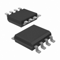
IR2520DSPBF International Rectifier, IR2520DSPBF Datasheet - Page 10

IR2520DSPBF
Manufacturer Part Number
IR2520DSPBF
Description
IC BALLAST CONTROL ADAPT 8SOIC
Manufacturer
International Rectifier
Type
Ballast Controllerr
Datasheet
1.IR2520DSTRPBF.pdf
(17 pages)
Specifications of IR2520DSPBF
Frequency
34 ~ 86 kHz
Current - Supply
10mA
Current - Output
230mA
Voltage - Supply
12.6 V ~ 15.4 V
Operating Temperature
-25°C ~ 125°C
Package / Case
8-SOIC (3.9mm Width)
Device Type
MOSFET
Module Configuration
Half Bridge
Peak Output Current
230mA
Supply Voltage Range
11.4V To 13.8V
Driver Case Style
DIP
No. Of Pins
8
Rohs Compliant
Yes
Lead Free Status / RoHS Status
Lead free / RoHS Compliant
Other names
*IR2520DSPBF
Available stocks
Company
Part Number
Manufacturer
Quantity
Price
IR2520D(S)& (PbF)
over-current fault. By using the RDSon of the external low-
side MOSFET for current sensing and the VS-sensing
circuitry, the IR2520D eliminates the need for an additional
current sensing resistor, filter and current-sensing pin. To
cancel changes in the RDSon value due to temperature and
MOSFET variations, the IR2520D performs a crest factor
measurement that detects when the peak current exceeds
the average current by a factor of 5 (CSCF). Measuring the
crest factor is ideal for detecting when the inductor saturates
due to excessive current that occurs in the resonant tank
when the frequency sweeps through resonance and the
lamp does not ignite. When the VCO voltage ramps up for
the first time from zero, the resonant tank current and
voltages increase as the frequency decreases towards
resonance (Figure 8). If the lamp does not ignite, the inductor
current will eventually saturate but the crest factor fault
protection is not active until the VCO voltage exceeds 4.8V
(V
decreasing to the capacitive side of resonance towards
the minimum frequency setting and the resonant tank current
and voltages will decrease again. When the VCO voltage
exceeds 4.8V (V
the non-ZVS protection and crest factor protection are both
enabled. The non-ZVS protection will increase the
frequency again cycle-by-cycle towards resonance from
the capacitive side. The resonant tank current will increase
again as the frequency nears resonance until the inductor
saturates again.
The crest factor protection is now enabled and measures
the instantaneous voltage at the VS pin only during the time
when LO is ‘high’ and after an initial 1us blank time from the
rising edge of LO. The blank time is necessary to prevent
the crest factor protection circuit from reacting to a non-
ZVS condition. An internal averaging circuit averages the
instantaneous voltage at the VS pin over 10 to 20 switching
cycles of LO. During Run Mode, the first time the inductor
saturates when LO is ‘high’ (after the 1us blank time) and
the peak current exceeds the average by 5 (CSCF), the
IR2520D will enter Fault Mode and both LO and HO outputs
will be latched ‘low’. The half-bridge will be safely disabled
before any damage can occur to the ballast components.
The crest factor peak-to-average fault factor varies as a
function of the internal average (Figure 20). The maximum
internal average should be below 3.0 volts. Should the
average exceed this amount, the multiplied average voltage
can exceed the maximum limit of the VS sensing circuit and
the VS sensing circuit will no longer detect crest factor
10
VCO_RUN
) for the first time. The frequency will continue
VCO_RUN
), the IC enters Run Mode and
V VCO
faults. This can occur when a half-bridge MOSFET is
selected that has an RDSon that is too large for the application
causing the internal average to exceed the maximum limit.
FAULT MODE
During Run Mode, should the VCO voltage decrease below
0.82V (V
will enter Fault Mode (see State Diagram). The LO and HO
gate driver outputs are both latched ‘low’ so that the half-
bridge is disabled. The VCO pin is pulled low to COM and
the FMIN pin decreases from 5V to COM. VCC draws
micro-power current (I
clamp voltage and the IC remains in Fault Mode without the
need for the charge-pump auxiliary supply. To exit Fault
Mode and return to Frequency Sweep Mode, VCC must be
cycled below the UVLO- threshold and back above the
UVLO+ threshold.
4.6V
I L
Fig. 8 Crest factor protection timing diagram
VCOSD
INDUCTIVE SIDE
OF RESONANCE
FREQUENCY SWEEP MODE
) or a crest factor fault occur, the IR2520D
CCFLT
) so that VCC stays at the
AVG*5
I MLS
CAPACITIVE SIDE
OF RESONANCE
LO
RUN MODE
www.irf.com
saturation
Inductor
FAULT MODE


