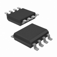
IR2520DSPBF International Rectifier, IR2520DSPBF Datasheet - Page 8

IR2520DSPBF
Manufacturer Part Number
IR2520DSPBF
Description
IC BALLAST CONTROL ADAPT 8SOIC
Manufacturer
International Rectifier
Type
Ballast Controllerr
Datasheet
1.IR2520DSTRPBF.pdf
(17 pages)
Specifications of IR2520DSPBF
Frequency
34 ~ 86 kHz
Current - Supply
10mA
Current - Output
230mA
Voltage - Supply
12.6 V ~ 15.4 V
Operating Temperature
-25°C ~ 125°C
Package / Case
8-SOIC (3.9mm Width)
Device Type
MOSFET
Module Configuration
Half Bridge
Peak Output Current
230mA
Supply Voltage Range
11.4V To 13.8V
Driver Case Style
DIP
No. Of Pins
8
Rohs Compliant
Yes
Lead Free Status / RoHS Status
Lead free / RoHS Compliant
Other names
*IR2520DSPBF
Available stocks
Company
Part Number
Manufacturer
Quantity
Price
IR2520D(S)& (PbF)
Fig. 4 Resonant tank Bode plot with lamp operating
V VCO
Vout
0.85V
Freq
Vin
8
fmax
4.8V
fmin
Fig. 3 IR2520D Frequency sweep mode timing
6V
Low -Q
Frequency Sweep Mode
High -Q
fmin
Run
diagram.
points.
Ignition
fmax
Start
Run Mode
Frequency
Run Mode
The IR2520D enters RUN mode when the voltage on pin
VCO exceeds 4.8V (V
the ballast output stage becomes a low-Q, series-L, paral-
lel-RC circuit. Also, the VS sensing and fault logic blocks
(Figure 5) both become enabled for protection against non-
ZVS and over-current fault conditions. The voltage on the
VCO pin continues to increase and the frequency deceases
further until the VCO pin voltage limits at 6V (V
and the minimum frequency is reached. The resonant in-
ductor, resonant capacitor, DC bus voltage and minimum
frequency determine the running lamp power. The IC stays
at this minimum frequency unless non-ZVS occurs at the
VS pin, a crest factor over-current condition is detected at
the VS pin, or VCC decreases below the UVLO- threshold
(see State Diagram).
Non Zero-Voltage Switching (ZVS) Protection
During run mode, if the voltage at the VS pin has not slewed
entirely to COM during the dead-time such that there is
voltage between the drain and source of the external low-
side half-bridge MOSFET when LO turns-on, then the system
is operating too close to, or, on the capacitive side of,
resonance. The result is non-ZVS capacitive-mode
switching that causes high peak currents to flow in the
half-bridge MOSFETs that can damage or destroy them
(Figure 6). This can occur due to a lamp filament failure(s),
DCBUS(+)
DCBUS(-)
RSUPPLY
CVCC
RFMIN
CVCO
Fig. 5 IR2520D Run mode circuitry.
COM
FMIN
VCC
VCO
1
2
3
4
CLAMP
15.6V
Bootstrap
VCO
Driver
Fault
Logic
FET
VCO_RUN
Driver
Sense
High-
Low-
and
side
VS
DCP2
8
7
6
5
). The lamp has ignited and
HO
VB
VS
LO
CBS
MLS
MHS
CSNUB
DCP1
www.irf.com
VCO_MAX
TO LOAD
LOAD RETURN
)


