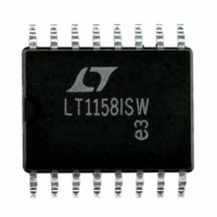
LT1158ISW#PBF Linear Technology, LT1158ISW#PBF Datasheet - Page 12

LT1158ISW#PBF
Manufacturer Part Number
LT1158ISW#PBF
Description
IC MOSFET DRVR 1/2BRDG NCH16SOIC
Manufacturer
Linear Technology
Datasheet
1.LT1158CNPBF.pdf
(22 pages)
Specifications of LT1158ISW#PBF
Configuration
Half Bridge
Input Type
PWM
Current - Peak
500mA
Number Of Configurations
1
Number Of Outputs
2
High Side Voltage - Max (bootstrap)
56V
Voltage - Supply
5 V ~ 30 V
Operating Temperature
-40°C ~ 85°C
Mounting Type
Surface Mount
Package / Case
16-SOIC (0.300", 7.5mm Width)
Lead Free Status / RoHS Status
Lead free / RoHS Compliant
Delay Time
-
Available stocks
Company
Part Number
Manufacturer
Quantity
Price
LT1158
APPLICATIONS INFORMATION
One fundamental difference in the operation of a step-
down regulator with synchronous switching is that it
never becomes discontinuous at light loads. The induc-
tor current doesn’t stop ramping down when it reaches
zero, but actually reverses polarity resulting in a constant
ripple current independent of load. This does not cause
any effi ciency loss as might be expected, since the nega-
tive inductor current is returned to V
turns back on.
The LT1158 performs the synchronous MOSFET drive
and current sense functions in a step-down switching
regulator. A reference and PWM are required to complete
the regulator. Any voltage-mode PWM controller may be
used, but the LT3525 is particularly well suited to high
power, high effi ciency applications such as the 10A circuit
shown in Figure 13. In higher current regulators a small
Schottky diode across the bottom MOSFET helps to reduce
reverse-recovery switching losses.
The LT1158 input pin can also be driven directly with a
ramp or sawtooth. In this case, the DC level of the input
waveform relative to the 1.4V threshold sets the LT1158
duty cycle. In the 5V to 3.3V converter circuit shown in
Figure 11, an LT1431 controls the DC level of a triangle wave
generated by a CMOS 555. The Figure 10 and 12 circuits
use an RC network to ramp the LT1158 input back up to
its 1.4V threshold following each switch cycle, setting a
constant off time. Figure 4 shows the effi ciency vs output
current for the Figure 12 regulator with V
12
Figure 4. Typical Effi ciency Curve for Step-Down
Regulator with Synchronous Switch
100
60
90
80
70
0
0.5
1.0
OUTPUT CURRENT (A)
FIGURE 12 CIRCUIT
V
IN
1.5
= 12V
2.0
2.5
3.0
IN
3.5
LT1158 F04
when the switch
IN
4.0
= 12V.
Current Limit in Switching Regulator Applications
Current is sensed by the LT1158 by measuring the voltage
across a current shunt (low valued resistor). Normally, this
shunt is placed in the source lead of the top MOSFET (see
Short-Circuit Protection in Bridge Applications). However,
in step-down switching regulator applications, the remote
current sensing capability of the LT1158 allows the actual
inductor current to be sensed. This is done by placing
the shunt in the output lead of the inductor as shown in
Figure 3. Routing of the SENSE
is critical to prevent stray pickup. These traces must be
routed together at minimum spacing and use a Kelvin
connection at the shunt.
When the voltage across R
LT1158 FAULT pin begins to conduct. By feeding the FAULT
signal back to a control input of the PWM, the LT1158 will
assume control of the duty cycle forming a true current
mode loop to limit the output current:
In LT3525 based circuits, connecting the FAULT pin to
the LT3525 soft-start pin accomplishes this function. In
circuits where the LT1158 input is being driven with a ramp
or sawtooth, the FAULT pin is used to pull down the DC
level of the input.
The constant off-time circuits shown in Figures 10 and 12
are unique in that they also use the current sense during
normal operation. The LT1431 output reduces the normal
LT1158 110mV fault conduction threshold such that the
FAULT pin conducts at the required load current, thus
discharging the input ramp capacitor. In current limit the
LT1431 output turns off, allowing the fault conduction
threshold to reach its normal value.
The resistor R
output voltage overshoot due to charge coupled into the
gate of the top MOSFET by a large start-up dv/dt on V
If DC operation of the top MOSFET is required, R
be 330k or greater to prevent loading the charge pump.
I
OUT
=
110mV
R
SENSE
GS
shown in Figure 3 is necessary to prevent
in current limit
SENSE
+
and SENSE
exceeds 110mV, the
–
PC traces
GS
must
1158fb
IN
.


