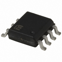
MIC4100YM Micrel Inc, MIC4100YM Datasheet - Page 14

MIC4100YM
Manufacturer Part Number
MIC4100YM
Description
IC DRIVER MOSFET 100V CMOS 8SOIC
Manufacturer
Micrel Inc
Datasheet
1.MIC4100YM.pdf
(18 pages)
Specifications of MIC4100YM
Configuration
Half Bridge
Input Type
Non-Inverting
Delay Time
27ns
Current - Peak
2A
Number Of Configurations
1
Number Of Outputs
2
High Side Voltage - Max (bootstrap)
118V
Voltage - Supply
9 V ~ 16 V
Operating Temperature
-40°C ~ 125°C
Mounting Type
Surface Mount
Package / Case
8-SOIC (3.9mm Width)
Device Type
MOSFET
Module Configuration
Half Bridge
Peak Output Current
2A
Output Resistance
3ohm
Input Delay
27ns
Output Delay
27ns
Supply Voltage Range
9V To 16V
Driver Case Style
SOIC
Lead Free Status / RoHS Status
Lead free / RoHS Compliant
Other names
576-1183
Available stocks
Company
Part Number
Manufacturer
Quantity
Price
Company:
Part Number:
MIC4100YM
Manufacturer:
Micrel Inc
Quantity:
135
Part Number:
MIC4100YM
Manufacturer:
MICREL/麦瑞
Quantity:
20 000
Company:
Part Number:
MIC4100YML
Manufacturer:
MAXIM
Quantity:
60
The power dissipated inside the MIC4100/1 is equal to the
ratio of Ron & Roff to the external resistive losses in Rg
and Rg_fet. Letting Ron =Roff, the power dissipated in the
MIC4100 due to driving the external MOSFET is:
Supply Current Power Dissipation
Power is dissipated in the MIC4100 even if is there i
nothing being driven. The supply current is drawn by the
bias for the internal circuitry, the level shifting circuitry and
shoot-through current in the output drivers. The supply
current is proportional to operating frequency and the Vdd
and Vhb voltages. The typical characteristic graphs show
how supply current varies with switching frequency and
supply voltage.
The power diss
current is
Total power dissipation and Thermal Considerations
Total power dissipation in the MIC4100 or MIC4101 i
equal to the power dissipation caused by driving the
external MOSFETs, the supply current and the internal
bootstrap diode.
The die temperature may be calculated once the total
power dissipation is known.
Propagation Delay and Delay Matching and other
Timing Considerations
Propagation delay and signal timing is an important
E
and
where
E
P
Qg
Vgs
fs
where
T
T
Pdiss
θ
P
Micrel, Inc.
March 2006
driver
driver
A
J
JC
dirver
driver
is
is
is
is
is
is
the
the
Pdiss
the
is
total
the
the
=
is
=
:
the
the
switching
Qg
Qg
the
junction t
is
maximum
total
thermal
Pdiss
gate
the
power
×
×
energy
Pdiss
total
V
V
gate
gs
power
gs
to
×
drive
=
source
resistance
dissipated
frequency
emperature
T
sup
fs
charge
dissipated
ipated by the MIC4100 due to supply
Pdiss
ambient te
J
dissipatio
=
ply
=
P
voltage
T
=
driver
at
sup
A
Vdd
from
Vgs
of
+
by
ply
per
(
mperature
°
Pdiss
n
Ron
the
C)
switching
on the
+
of
×
junction t
switching
Pdiss
gate
Idd
the
+
total
MOSFET
MIC4100/1
Rg
drive
+
Ron
drive
the
×
Vhb
o
cycle
+
θ
ambient
circuit
MOSFET
JA
Rg
+
×
Pdiode
_
Ihb
fet
air
on
(
°
total
C/W)
and
off
s
s
14
consideration in a high performance power supply. The
MIC4100 is designed no
delay but to minimize the mismatch in delay between the
high-side and low-side drivers.
Fast propagation delay between the input and output drive
waveform is desirable. It improves overcurrent protection
by decreasing the response
signal
propagation delay also minimizes phase shift errors in
power supplies with wide bandwidth control loops.
Many power supply topologies use two switching
MOSFETs operating 180º out of phase from each other.
These MOSFETs must not be on at the same tim
short circuit will occur, causing high peak currents and
higher power dissipation in the MOSFETs. The MIC4100
and MIC4101 output gate drivers are not designed with
anti-shoot-through protection circuitry. The output drives
signals simply follow the inputs. The power supply design
must include timing delays (dead-time) between the input
signals to prevent shoot-through. The MIC4100 &
MIC4101 drivers specify delay matching between the two
drivers to help improve power supply performance by
reducing the amount of dead-time required between the
input signals.
Care must be taken to insure the input signal pulse width
is greater than the minimum specified pulse width. An
input signal tha
result in no output pulse or an output pulse whose width is
significantly less than the input.
The maximum duty cycle (ratio of high side on-time to
switching period) is controlled by the minimum pulse width
of the low side and by the t
capacitor to charge during the off-time. Adequate time
must be allowed for the C
the high-side driver is turned on.
Decoupling and Bootstrap Capacitor Selection
Decoupling capacitors are requir
(Vdd) and high side (HB) supply pins. These capacitors
supply the charge necessary to drive the
MOSFETs as well as minimize the voltage ripple on these
pins. The capacitor from HB to HS serves double duty by
providing decoupling for the high-side circuitry as well as
providing current to the high-side circuit while the high-side
external
recommended because of their low impedance and small
size. Z5U type ceramic capacitor dielectrics are not
recommended due to the large change in capacitance over
temperature and voltage. A minimum value of 0.1uf is
required for each of the capacitors, regardless of the
MOSFETs being driven. Larger MOSFETs may require
larger capacitance values for proper operation. The
voltage rating of the capacitors depends on the supply
voltage, ambient temperature and the voltage derating
used for reliability. 25V rated X5R or X7R ceramic
and
MOSFET
the
t is less than the minimum pulse width may
MOSFET
is
t only to minimize propagation
on.
B
capacitor to charge up before
time between the control
Ceramic
ime required for the C
gate
ed for both the low side
drive.
capacitors
M9999-031506
MIC4100/1
Minimizing
external
e or a
are
B


