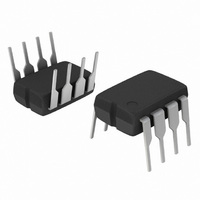
NCP5106BPG ON Semiconductor, NCP5106BPG Datasheet - Page 4

NCP5106BPG
Manufacturer Part Number
NCP5106BPG
Description
IC DRIVER HI/LO 600V 8-DIP
Manufacturer
ON Semiconductor
Type
High Side/Low Sider
Datasheet
1.NCP5106BDR2G.pdf
(18 pages)
Specifications of NCP5106BPG
Configuration
High and Low Side, Synchronous
Input Type
Non-Inverting
Delay Time
100ns
Current - Peak
250mA
Number Of Configurations
1
Number Of Outputs
2
High Side Voltage - Max (bootstrap)
600V
Voltage - Supply
10 V ~ 20 V
Operating Temperature
-40°C ~ 125°C
Mounting Type
Through Hole
Package / Case
8-DIP (0.300", 7.62mm)
Rise Time
160 ns
Fall Time
75 ns
Supply Voltage (min)
- 0.3 V
Supply Current
5 mA
Maximum Operating Temperature
+ 150 C
Mounting Style
Through Hole
Bridge Type
Full Bridge, Half Bridge
Minimum Operating Temperature
- 55 C
Number Of Drivers
2
Lead Free Status / RoHS Status
Lead free / RoHS Compliant
Other names
NCP5106BPGOS
Available stocks
Company
Part Number
Manufacturer
Quantity
Price
Part Number:
NCP5106BPG
Manufacturer:
ON/安森美
Quantity:
20 000
Stresses exceeding Maximum Ratings may damage the device. Maximum Ratings are stress ratings only. Functional operation above the
Recommended Operating Conditions is not implied. Extended exposure to stresses above the Recommended Operating Conditions may affect
device reliability.
MAXIMUM RATINGS
V
BOOT−
V
dV
CC_transient
V
V
V
V
Rating
BRIDGE
V
T
BRIDGE
BRIDGE
DRV_LO
DRV_HI
R
V
J_max
IN_XX
T
qJA
CC
ST
V
BRIDGE
/dt
Main power supply voltage
Main transient power supply voltage:
VHV: High Voltage BRIDGE pin
Allowable Negative Bridge Pin Voltage for IN_LO Signal Propagation to DRV_LO
(see characterization curves for detailed results)
VHV: Floating supply voltage
VHV: High side output voltage
Low side output voltage
Allowable output slew rate
Inputs IN_HI, IN_LO
ESD Capability:
− HBM model (all pins except pins 6−7−8 in 8 pins
− Machine model (all pins except pins 6−7−8 in 8 pins
Latch up capability per JEDEC JESD78
Power dissipation and Thermal characteristics
PDIP−8: Thermal Resistance, Junction−to−Air
SO−8: Thermal Resistance, Junction−to−Air
Storage Temperature Range
Maximum Operating Junction Temperature
IV
package or 11−12−13 in 14 pins package)
package or 11−12−13 in 14 pins package)
CC_max
= 5 mA during 10 ms
Symbol
http://onsemi.com
4
−0.3 to V
−1.0 to V
V
BRIDGE
V
−55 to +150
−0.3 to 20
−0.3 to 20
−1 to 600
BOOT
Value
+150
−10
200
100
178
23
50
2
CC
CC
− 0.3 to
+ 0.3
+ 0.3
+ 0.3
°C/W
V/ns
Unit
kV
°C
°C
V
V
V
V
V
V
V
V
V


