IRS26302DJPBF International Rectifier, IRS26302DJPBF Datasheet - Page 9
IRS26302DJPBF
Manufacturer Part Number
IRS26302DJPBF
Description
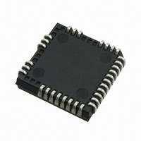
IC BRIDGE +1 GATE DVR 3PH 44PLCC
Manufacturer
International Rectifier
Datasheet
1.IRS26302DJTRPBF.pdf
(51 pages)
Specifications of IRS26302DJPBF
Configuration
3 Phase Bridge
Input Type
Non-Inverting
Delay Time
320ns
Current - Peak
200mA
Number Of Configurations
1
Number Of Outputs
3
High Side Voltage - Max (bootstrap)
600V
Voltage - Supply
10 V ~ 20 V
Operating Temperature
-40°C ~ 125°C
Mounting Type
Surface Mount
Package / Case
44-PLCC (32 Leads)
Number Of Drivers
6
Driver Configuration
Non-Inverting
Driver Type
High and Low Side
Input Logic Level
CMOS/TTL
Rise Time
190ns
Fall Time
75ns
Propagation Delay Time
710ns
Peak Output Current
350mA
Power Dissipation
4.6W
Operating Supply Voltage (min)
10V
Turn Off Delay Time
50ns
Turn On Delay Time (max)
50ns
Operating Temp Range
-40C to 125C
Operating Temperature Classification
Automotive
Mounting
Surface Mount
Pin Count
32
Package Type
PLCC
Lead Free Status / RoHS Status
Lead free / RoHS Compliant
Available stocks
Company
Part Number
Manufacturer
Quantity
Price
Company:

Part Number:
IRS26302DJPBF
Manufacturer:
International Rectifier
Quantity:
10 000


Static Electrical Characteristics (continued)
(V
to V
COM and are applicable to the respective output leads HO or LO. The V
The V
applicable to PFCout/BRout lead.
V
V
Ron_RCIN
IPFC
www.irf.com
IPFC
Symbol
PFCH
IqVdcon
IqVdcoff
PFCL
IBR
CC
PFCI
IBR
PFCI
R
BRI
BRI
I
IEN
I
RBS
I
ON_FLT
ITRIP+
ITRIP-
SS
I
RCIN
-COM) = (V
I
IN+
IN-
TRIP+
TRIP-
TRIP+
/V
/V
TRIP
BSUV
O+
O-
IN
O+
O-
and are applicable to all six channels. The VO and IO parameters are referenced to respective V
BRH
BRL
/
/
/
/
parameters are referenced to V
Definition
Output high short circuit pulsed current,
PFC
Output low short circuit pulsed current,
PFC
High level output voltage, V
PFC
low level output voltage, V
Input bias current LIN1,2,3, HIN1,2,3,
PFC
Input bias current LIN1,2,3, HIN1,2,3,
PFC
ITRIP input bias current
ITRIP input bias current
PFC
PFC
RCIN input bias current
EN input bias current
RCIN low on resistance
FLT low on resistance
Ron internal bootstrap diode
Quiescent VDC supply current on status
Quiescent VDC supply current off status
B
-V
S
OUT
OUT
OUT
IN
IN
TRIP
TRIP
) = 15 V. TA = 25
/BR
/BR
/BR
/BR
/BR
/BR
/BR
IN,
IN,
OUT
OUT
OUT
(OUT=HI)
(OUT=LO)
TRIP
TRIP
input bias current
input bias current
° C
O
BIAS
, PFC
unless otherwise specified. The VIN and IIN parameters are referenced
S
– V
. The PFCIo/BRIo and VPFC/ VBR are referenced to V
OUT
O
,
/BR
OUT
9
Min
120
210
350
100
100
—
—
—
—
—
—
—
—
—
—
—
—
Typ
250
430
900
400
200
200
200
20
50
50
—
0
1
0
0
0
0
CCUV
1400
Max
600
860
100
100
300
300
—
—
—
—
1
2
5
5
5
1
parameters are referenced to V
Units
mA
mV
µA
µA
P
VDC = Vgf , VDC + = 40- 600 V
P
© 2009 International Rectifier
FCOUT
FCOUT
IRS26302DJ
VDC - Vgf = 250 mV,
V
Test Conditions
VDC+ = 40 -600 V
PFCTRIP
= 15 V, PW </= 10 us
V
= 0 V, PW </= 10 us
V
V
V
PFCTRIP
V
I
V
RCIN
I = 1.5 mA
I = 1.5 mA
O
ITRIP
ITRIP
V
EN
IN
= 20 mA
IN
= 3.3 V
= 3.3V
= 0 V
=-250 mV
SS
= 15 V
= 1 V
= 0 V
= 0 V
and are
S
and
SS
.
Related parts for IRS26302DJPBF
Image
Part Number
Description
Manufacturer
Datasheet
Request
R

Part Number:
Description:
SCHOTTKY RECTIFIER
Manufacturer:
International Rectifier Corp.
Datasheet:
Part Number:
Description:
SCHOTTKY RECTIFIER
Manufacturer:
International Rectifier Corp.
Datasheet:
Part Number:
Description:
SCHOTTKY RECTIFIER
Manufacturer:
International Rectifier Corp.
Datasheet:
Part Number:
Description:
SCHOTTKY RECTIFIER
Manufacturer:
International Rectifier Corp.
Datasheet:
Part Number:
Description:
SCHOTTKY RECTIFIER
Manufacturer:
International Rectifier Corp.
Datasheet:
Part Number:
Description:
SCHOTTKY RECTIFIER
Manufacturer:
International Rectifier Corp.
Datasheet:
Part Number:
Description:
SCHOTTKY RECTIFIER
Manufacturer:
International Rectifier Corp.
Datasheet:
Part Number:
Description:
SCHOTTKY RECTIFIER
Manufacturer:
International Rectifier Corp.
Datasheet:
Part Number:
Description:
SCHOTTKY RECTIFIER
Manufacturer:
International Rectifier Corp.
Datasheet:
Part Number:
Description:
SCHOTTKY RECTIFIER
Manufacturer:
International Rectifier Corp.
Datasheet:
Part Number:
Description:
SCHOTTKY RECTIFIER
Manufacturer:
International Rectifier Corp.
Datasheet:
Part Number:
Description:
SCHOTTKY RECTIFIER
Manufacturer:
International Rectifier Corp.
Datasheet:
Part Number:
Description:
SCHOTTKY RECTIFIER
Manufacturer:
International Rectifier Corp.
Datasheet:
Part Number:
Description:
SCHOTTKY RECTIFIER
Manufacturer:
International Rectifier Corp.
Datasheet:
Part Number:
Description:
SCHOTTKY RECTIFIER
Manufacturer:
International Rectifier Corp.
Datasheet: