VLA500-01 Powerex Inc, VLA500-01 Datasheet - Page 2
VLA500-01
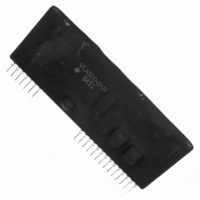
Manufacturer Part Number
VLA500-01
Description
IC IGBT GATE DVR/DC-DC CONV 12A
Manufacturer
Powerex Inc
Datasheet
1.VLA500-01.pdf
(7 pages)
Specifications of VLA500-01
Configuration
Low-Side
Input Type
Non-Inverting
Delay Time
600ns
Current - Peak
12A
Number Of Configurations
1
Number Of Outputs
1
Voltage - Supply
14.2 V ~ 15.8 V
Operating Temperature
-20°C ~ 60°C
Mounting Type
Through Hole
Package / Case
21-SIP Module
Device Type
IGBT
Peak Reflow Compatible (260 C)
Yes
Supply Voltage Max
16.5V
Source Output Current Max
12A
Leaded Process Compatible
No
No. Of Drivers
1
Lead Free Status / RoHS Status
Lead free / RoHS Compliant
For Use With
BG2A-NF - KIT DEV BOARD FOR IGBT
High Side Voltage - Max (bootstrap)
-
Lead Free Status / RoHS Status
Lead free / RoHS Compliant, Lead free / RoHS Compliant
Other names
835-1063
Available stocks
Company
Part Number
Manufacturer
Quantity
Price
Company:

Part Number:
VLA500-01R
Manufacturer:
MICROCHIP
Quantity:
1 001
Part Number:
VLA500-01R
Manufacturer:
MIT
Quantity:
20 000


2
Powerex, Inc., 200 E. Hillis Street, Youngwood, Pennsylvania 15697-1800 (724) 925-7272
VLA500-01
Hybrid IC IGBT Gate Driver +
DC/DC Converter
Absolute Maximum Ratings, T
Characteristics
Supply Voltage, DC
Input Signal Voltage (Applied between Pin 6 - 7, 50% Duty Cycle, Pulse Width 1ms)
Output Voltage (When the Output Voltage is "H")
Output Current
(Pulse Width 2µs)
Isolation Voltage (Sine Wave Voltage 60HZ, for 1 Minute)
Case Temperature1 (Surface Temperature Opto-coupler Location)***
Case Temperature2 (Surface Temperature Except Opto-coupler Location)
Operating Temperature (No Condensation Allowable)
Storage Temperature (No Condensation Allowable)
Fault Output Current (Applied Pin 28)
Input Voltage to Pin 30 (Applied Pin 30)
Gate Drive Current (Average)
*Differs from temperature cycle condition.
**Refer to I
***T
Electrical and Mechanical Characteristics, T
Characteristics
Supply Voltage
Pull-up Voltage on Input Side
"H" Input Current
Switching Frequency
Gate Resistance
"H" Input Current
Gate Positive Supply Voltage
Gate Negative Supply Voltage
Gate Supply Efficiency
"H" Output Voltage
"L" Output Voltage
"L-H" Propagation Time
"L-H" Rise Time
"H-L" Propagation Time
"H-L" Fall Time
C1
Measurement Point (opto-coupler location)
drive
VS. T
a
CHARACTERISTICS (TYPICAL) graph. (Needs Derating)
a
= 25°C unless otherwise specified
Symbol
V
t
t
V
V
V
V
R
E
PLH
PHL
V
I
I
OH
IH
IH
CC
EE
OL
t
t
IN
f
ta
D
G
r
f
E
ta
10kW Connected Between Pin 23-20
10kW Connected Between Pin 23-20
a
= (V
= 25°C unless otherwise specified, V
CC
Load Current = 210mA
Recommended Range
Recommended Range
Recommended Range
Recommended Range
Recommended Range
+ |V
(OPTO-COUPLER LOCATION)
EE
I
I
I
I
T C1 MEASUREMENT POINT
IH
IH
IH
IH
V
|) x 0.21 / (15 x I
IN
Test Conditions
= 16mA
= 16mA
= 16mA
= 16mA
—
—
= 5V
MARKING SIDE
Symbol
D
V
I
V
I
I
T
T
T
T
OHP
drive
) x 100
OLP
I
V
V
FO
R30
V
ISO
opr
C1
C2
stg
D
O
i
D
Min.
14.2
4.75
15.2
15.2
-5.5
0.3
0.6
60
14
—
—
—
—
= 15V, R
-6
1
-25 to 100*
VLA500-01
-1 ~ 16.5
-20 to 60
-1 ~ 7
210**
2500
V
100
-12
12
85
20
50
CC
15.3
Typ.
G
0.6
0.3
0.3
15
16
—
—
16
—
—
75
—
5
1
= 2.2 W)
-11.5
Max.
15.8
5.25
17.5
16.5
-11
1.3
19
20
—
—
—
1
1
1
Amperes
Amperes
Volts
Volts
Volts
Volts
Rev. 2/08
Units
V
mA
mA
°C
°C
°C
°C
rms
Volts
Volts
Volts
Volts
Volts
Volts
Units
kHz
mA
mA
µs
µs
µs
µs
%
W
Related parts for VLA500-01
Image
Part Number
Description
Manufacturer
Datasheet
Request
R

Part Number:
Description:
Manufacturer:
Powerex Inc
Datasheet:
Part Number:
Description:
Manufacturer:
Powerex Inc
Datasheet:
Part Number:
Description:
Manufacturer:
Powerex Inc
Datasheet:
Part Number:
Description:
Manufacturer:
Powerex Inc
Datasheet:
Part Number:
Description:
Manufacturer:
Powerex Inc
Datasheet:
Part Number:
Description:
Manufacturer:
Powerex Inc
Datasheet:
Part Number:
Description:
Manufacturer:
Powerex Inc
Datasheet:
Part Number:
Description:
Manufacturer:
Powerex Inc
Datasheet:
Part Number:
Description:
Manufacturer:
Powerex Inc
Datasheet:
Part Number:
Description:
Manufacturer:
Powerex Inc
Datasheet:
Part Number:
Description:
Manufacturer:
Powerex Inc
Datasheet:
Part Number:
Description:
Manufacturer:
Powerex Inc
Datasheet:
Part Number:
Description:
Manufacturer:
Powerex Inc
Datasheet:
Part Number:
Description:
Manufacturer:
Powerex Inc
Datasheet: