VLA500-01 Powerex Inc, VLA500-01 Datasheet - Page 5
VLA500-01
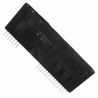
Manufacturer Part Number
VLA500-01
Description
IC IGBT GATE DVR/DC-DC CONV 12A
Manufacturer
Powerex Inc
Datasheet
1.VLA500-01.pdf
(7 pages)
Specifications of VLA500-01
Configuration
Low-Side
Input Type
Non-Inverting
Delay Time
600ns
Current - Peak
12A
Number Of Configurations
1
Number Of Outputs
1
Voltage - Supply
14.2 V ~ 15.8 V
Operating Temperature
-20°C ~ 60°C
Mounting Type
Through Hole
Package / Case
21-SIP Module
Device Type
IGBT
Peak Reflow Compatible (260 C)
Yes
Supply Voltage Max
16.5V
Source Output Current Max
12A
Leaded Process Compatible
No
No. Of Drivers
1
Lead Free Status / RoHS Status
Lead free / RoHS Compliant
For Use With
BG2A-NF - KIT DEV BOARD FOR IGBT
High Side Voltage - Max (bootstrap)
-
Lead Free Status / RoHS Status
Lead free / RoHS Compliant, Lead free / RoHS Compliant
Other names
835-1063
Available stocks
Company
Part Number
Manufacturer
Quantity
Price
Company:

Part Number:
VLA500-01R
Manufacturer:
MICROCHIP
Quantity:
1 001
Part Number:
VLA500-01R
Manufacturer:
MIT
Quantity:
20 000


Powerex, Inc., 200 E. Hillis Street, Youngwood, Pennsylvania 15697-1800 (724) 925-7272
VLA500-01
Hybrid IC IGBT Gate Driver +
DC/DC Converter
Application Circuit
Rev. 2/08
Common
Control
+15V
Fault
+5V
Component Selection:
Design
D1
DZ1
DZ2, DZ3
C1
C2, C3
C4
CS
C trip
R1
R2
R3
R4
OP1
B1
Notes:
(1) The V CE detection diode should have a blocking voltage rating equal to or greater than the V CES of the IGBT
(2) DZ1 is necessary to protect Pin 30 of the driver from voltage surges during the recovery of D1.
(3) Power supply input and output decoupling capacitors should be connected as close as possible to the pins of the gate driver.
(4) DC-to-DC converter output decoupling capacitors must be sized to have appropriate ESR and ripple current
1
being driven. Recovery time should be less than 200ns to prevent application of high voltage to Pin 30.
capability for the IGBT being driven.
2
+
B1
3
C1
4
Typical Value
0.5A
30V, 0.5W
18V, 1.0W
150µF, 35V
100-1000µF, 35V
0.01µF
0-1000pF
0-200pF
4.7kΩ, 0.25W
3.3kΩ, 0.25W
1kΩ, 0.25W
4.7kΩ, 0.25W
NEC PS2501
CMOS Buffer
5
6
7
R4
C4
R3
Description
V CE detection diode – fast recovery, V rrm > V CES of IGBT being used (Note 1)
Detect input pin surge voltage protection (Note 2)
Gate surge voltage protection
V D supply decoupling – Electrolytic, long life, low Impedance, 105°C (Note 3)
DC/DC output filter – Electrolytic, long life, low Impedance, 105°C (Note 3,4)
Fault feedback signal noise filter
Adjust soft shutdown – Multilayer ceramic or film (see application note)
Adjust trip time – Multilayer ceramic or film (see application note)
Fault sink current limiting resistor
Fault signal noise suppression resistor
Fault feedback signal noise filter
Fault feedback signal pull-up
Opto-coupler for fault feedback signal isolation
74HC04 or similar – Must actively pull high to maintain noise immunity
VLA500-01
OP1
R1
17 18 19 20 21 22
R2
C2
+
23 24 25
+
C3
26 27
R G
CS
28
C trip
29
DZ2
DZ3
30
DZ1
G
E
D1
IGBT MODULE
5
Related parts for VLA500-01
Image
Part Number
Description
Manufacturer
Datasheet
Request
R

Part Number:
Description:
Manufacturer:
Powerex Inc
Datasheet:
Part Number:
Description:
Manufacturer:
Powerex Inc
Datasheet:
Part Number:
Description:
Manufacturer:
Powerex Inc
Datasheet:
Part Number:
Description:
Manufacturer:
Powerex Inc
Datasheet:
Part Number:
Description:
Manufacturer:
Powerex Inc
Datasheet:
Part Number:
Description:
Manufacturer:
Powerex Inc
Datasheet:
Part Number:
Description:
Manufacturer:
Powerex Inc
Datasheet:
Part Number:
Description:
Manufacturer:
Powerex Inc
Datasheet:
Part Number:
Description:
Manufacturer:
Powerex Inc
Datasheet:
Part Number:
Description:
Manufacturer:
Powerex Inc
Datasheet:
Part Number:
Description:
Manufacturer:
Powerex Inc
Datasheet:
Part Number:
Description:
Manufacturer:
Powerex Inc
Datasheet:
Part Number:
Description:
Manufacturer:
Powerex Inc
Datasheet:
Part Number:
Description:
Manufacturer:
Powerex Inc
Datasheet: