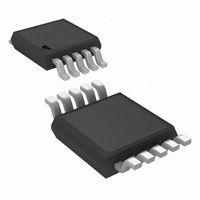
LM5106MMX/NOPB National Semiconductor, LM5106MMX/NOPB Datasheet

LM5106MMX/NOPB
Specifications of LM5106MMX/NOPB
Available stocks
Related parts for LM5106MMX/NOPB
LM5106MMX/NOPB Summary of contents
Page 1
... Drives both a high side and low side N-channel MOSFET ■ 1.8A peak output sink current ■ 1.2A peak output source current Simplified Block Diagram © 2009 National Semiconductor Corporation LM5106 ■ Bootstrap supply voltage range up to 118V DC ■ Single TTL compatible Input ■ ...
Page 2
Connection Diagram Ordering Information Ordering Number Package Type LM5106MM LM5106MMX LM5106SD LM5106SDX Pin Descriptions Pin Name Description 1 VDD Positive gate drive supply 2 HB High side gate driver bootstrap rail 3 HO High side gate driver output 4 HS ...
Page 3
... Absolute Maximum Ratings If Military/Aerospace specified devices are required, please contact the National Semiconductor Sales Office/ Distributors for availability and specifications and – (Note Electrical Characteristics apply over the full operating junction temperature range. Unless otherwise specified, V 5V. No load HO. RDT= 100kΩ ...
Page 4
Switching Characteristics type apply over the full operating junction temperature range. Unless otherwise specified, V Load (Note 4). Symbol Parameter t Lower Turn-Off Propagation Delay LPHL t Upper Turn-Off Propagation Delay HPHL t Lower Turn-On Propagation ...
Page 5
Typical Performance Characteristics V Operating Current vs Frequency DD Quiescent Current vs Supply Voltage HB Operating Current vs Frequency Operating Current vs Temperature 20175910 Quiescent Current vs Temperature 20175912 HO & LO Peak Output Current vs Output Voltage 20175916 5 ...
Page 6
Undervoltage Rising Threshold vs Temperature LO & Low Level Output Voltage vs Temperature Input Threshold vs Temperature www.national.com Undervoltage Hysteresis vs Temperature 20175919 LO & High Level Output Voltage vs Temperature 20175921 Dead-Time vs RT Resistor ...
Page 7
Dead-Time vs Temperature (RT = 10k) Timing Diagrams FIGURE 3. LM5106 Switching Time Definitions: t Dead-Time vs Temperature (RT = 100k) 20175926 FIGURE 2. LM5106 Input - Output Waveforms LPLH 7 20175927 20175903 20175904 , ...
Page 8
FIGURE 4. LM5106 Enable: t Operational Notes The LM5106 is a single PWM input Gate Driver with Enable that offers a programmable dead-time. The dead-time is set with a resistor at the RDT pin and can be adjusted from 100ns ...
Page 9
HS must always lower potential than HO. Pulling HO more than -0.3V below HS can activate parasitic transistors resulting in excessive current flow from the HB supply, possibly resulting in damage to the IC. The same ...
Page 10
Physical Dimensions Notes: Unless otherwise specified 1. Standard lead finish to be 200 microinches/5.00 micrometers minimum tin/lead (solder) on copper. 2. Pin 1 identification to have half of full circle option JEDEC registration as of Feb. 2000. www.national.com ...
Page 11
Notes 11 www.national.com ...
Page 12
... For more National Semiconductor product information and proven design tools, visit the following Web sites at: Products Amplifiers www.national.com/amplifiers Audio www.national.com/audio Clock and Timing www.national.com/timing Data Converters www.national.com/adc Interface www.national.com/interface LVDS www.national.com/lvds Power Management www.national.com/power Switching Regulators www.national.com/switchers LDOs www.national.com/ldo LED Lighting www ...


