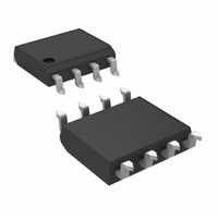
LM27222M/NOPB National Semiconductor, LM27222M/NOPB Datasheet - Page 7

LM27222M/NOPB
Manufacturer Part Number
LM27222M/NOPB
Description
IC MOSFET DVR SYNC 4.5A HS 8SOIC
Manufacturer
National Semiconductor
Datasheet
1.LM27222MXNOPB.pdf
(11 pages)
Specifications of LM27222M/NOPB
Configuration
High and Low Side, Synchronous
Input Type
PWM
Delay Time
14ns
Current - Peak
3A
Number Of Configurations
1
Number Of Outputs
2
High Side Voltage - Max (bootstrap)
30V
Voltage - Supply
4 V ~ 6.85 V
Operating Temperature
-40°C ~ 125°C
Mounting Type
Surface Mount
Package / Case
8-SOIC (3.9mm Width)
Number Of Drivers
2
Driver Configuration
Invert/Non-Invert
Driver Type
High and Low Side
Rise Time
17ns
Fall Time
14ns
Propagation Delay Time
8ns
Operating Supply Voltage (max)
6.85V
Peak Output Current
4.5mA
Power Dissipation
720mW
Operating Supply Voltage (min)
4V
Operating Temp Range
-40C to 125C
Operating Temperature Classification
Automotive
Mounting
Surface Mount
Pin Count
8
Package Type
SOIC N
Lead Free Status / RoHS Status
Lead free / RoHS Compliant
Other names
LM27222M
Application Information
GENERAL
The LM27222 is designed for high speed and high operating
reliability. The driver can handle very narrow, down to zero,
PWM pulses in a guaranteed, deterministic way. Therefore,
the HG and LG outputs are always in predictable states. No
latches are used in the HG and LG control logic so the
drivers cannot get "stuck" in the wrong state. The driver
design allows for powering up with a pre-biasing voltage
being present at the regulator output. To reduce conduction
losses in DC-DC converters with low duty factors the
LM27222 driver can be powered from a 6.5V
rail.
It is recommended to use the same power rail for both the
controller and driver. If two different power rails are used,
never allow the PWM pulse magnitude at the IN input or the
control voltage at the LEN input to be above the driver V
voltage or unpredictable HG and LG outputs pulse widths
may result.
MINIMUM PULSE WIDTH
As the input pulse width to the IN pin is decreased, the pulse
width of the high-side gate drive (HG-SW) also decreases.
However, for input pulse widths 60ns and smaller, the
HG-SW remains constant at 30ns. Thus the minimum pulse
width of the driver output is 30ns. Figure 5 shows an input
pulse at the IN pin 20ns wide, and the output of the driver, as
measured between the nodes HG and SW is a 30ns wide
pulse. Figure 6 shows the variation of the SW node pulse
width vs IN pulse width. At the IN pin, if a falling edge is
followed by a rising edge within 5ns, the HG may ignore the
rising edge and remain low until the IN pin toggles again. If a
rising edge is followed by a falling edge within 5ns, the pulse
may be completely ignored.
FIGURE 5. Min On Time
20117905
±
5% power
CC
7
ADAPTIVE SHOOT-THROUGH PROTECTION
The LM27222 prevents shoot-through power loss by ensur-
ing that both the high- and low-side MOSFETs are not con-
ducting at the same time. When the IN signal rises, LG is first
pulled down. The adaptive shoot-through protection circuit
waits for LG to reach 0.9V before turning on HG. Similarly,
when IN goes low, HG is pulled down first, and the circuit
turns LG on only after the voltage difference between the
high-side gate and the switch node, i.e. HG-SW, has fallen to
0.9V.
It is possible in some applications that at power-up the
driver’s SW pin is above 3V in either buck or boost com-
verter applications. For instance, in a buck configuration a
pre-biasing voltage can be either a voltage from anothert
power rail connected to the load, or a leakage voltage
through the load, or it can be an output capacitor pre-
charged above 3V while no significant load is present. In a
boost application it can be an input voltage rail above 3V.
In the case of insufficient initial CB-SW voltage (less than
2V) such as when the output rail is pre-biased, the shoot-
through protection circuit holds LG low for about 170ns,
beginning from the instant when IN goes high. After the
170ns delay, the status of LG is dictated by LEN and IN.
Once LG goes high and SW goes low, the bootstrap capaci-
tor will be charged up (assuming SW is grounded for long
enough time). As a result, CB-SW will be close to 5V and the
LM27222 will now fully support synchronous operation.
The dead-time between the high- and low-side pulses is kept
as small as possible to minimize conduction through the
body diode of the low-side MOSFET(s).
FIGURE 6.
20117906
www.national.com


