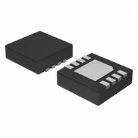
NCP3420MNR2G ON Semiconductor, NCP3420MNR2G Datasheet - Page 3

NCP3420MNR2G
Manufacturer Part Number
NCP3420MNR2G
Description
MOSFET DVR DUAL 1PH 12V 8-DFN
Manufacturer
ON Semiconductor
Datasheet
1.NCP3420MNR2G.pdf
(9 pages)
Specifications of NCP3420MNR2G
Configuration
High and Low Side, Synchronous
Input Type
Non-Inverting
Delay Time
30ns
Number Of Configurations
1
Number Of Outputs
2
High Side Voltage - Max (bootstrap)
12V
Voltage - Supply
4.6 V ~ 13.2 V
Operating Temperature
0°C ~ 85°C
Mounting Type
Surface Mount
Package / Case
8-TFDFN Exposed Pad
Lead Free Status / RoHS Status
Lead free / RoHS Compliant
Current - Peak
-
Lead Free Status / Rohs Status
Lead free / RoHS Compliant
Stresses exceeding Maximum Ratings may damage the device. Maximum Ratings are stress ratings only. Functional operation above the
Recommended Operating Conditions is not implied. Extended exposure to stresses above the Recommended Operating Conditions may affect
device reliability.
1. Internally limited by thermal shutdown, 150°C min.
2. 2 layer board, 1 in
3. 60−180 seconds minimum above 237°C.
NOTE:
NOTE:
MAXIMUM RATINGS
MAXIMUM RATINGS
Operating Ambient Temperature, T
Operating Junction Temperature, T
Package Thermal Resistance: SO−8
Package Thermal Resistance: DFN8 (Note 2)
Storage Temperature Range, T
Lead Temperature Soldering (10 sec): Reflow (SMD styles only)
JEDEC Moisture Sensitivity Level
Junction−to−Case, R
Junction−to−Ambient, R
Junction−to−Case, R
Junction−to−Ambient, R
Pin Symbol
This device is ESD sensitive. Use standard ESD precautions when handling.
All voltages are with respect to PGND except where noted.
PGND
DRVH
DRVL
BST
V
SW
OD
IN
CC
2
Cu, 1 oz thickness.
qJC
qJC
qJA
qJA
(From die to exposed pad)
(2−Layer Board)
S
Bootstrap Supply Voltage Input
DRVH and DRVL Control Input
Main Supply Voltage Input
(Bootstrap Supply Return)
A
High−Side Driver Output
J
Low−Side Driver Output
(Note 1)
Switching Node
Output Disable
Pin Name
Ground
Rating
http://onsemi.com
3
40 V v 50 ns wrt/PGND
35 V v 50 ns wrt/PGND
35 V wrt/PGND
40 V < 50 ns
15 V wrt/SW
BST + 0.3 V
15 V wrt/SW
V
CC
35 V DC
SO−8 (260 peak profile)
V
6.5 V
6.5 V
15 V
0 V
MAX
+ 0.3 V
Pb−Free (Note 3)
−2.0 V < 200 ns wrt/SW
−10 V < 200 ns
−5.0 V < 200 ns
−65 to 150
−0.3 V wrt/SW
−0.3 V wrt/SW
260 peak
0 to 150
0 to 85
−5.0 V DC
−0.3 V DC
Value
123
7.5
−0.3 V
−0.3 V
−0.3 V
45
55
1
V
0 V
MIN
°C/W
°C/W
°C/W
°C/W
Unit
°C
°C
°C
°C
−


