NCP3420MNR2G ON Semiconductor, NCP3420MNR2G Datasheet - Page 4
NCP3420MNR2G
Manufacturer Part Number
NCP3420MNR2G
Description
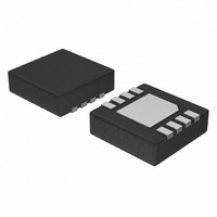
MOSFET DVR DUAL 1PH 12V 8-DFN
Manufacturer
ON Semiconductor
Datasheet
1.NCP3420MNR2G.pdf
(9 pages)
Specifications of NCP3420MNR2G
Configuration
High and Low Side, Synchronous
Input Type
Non-Inverting
Delay Time
30ns
Number Of Configurations
1
Number Of Outputs
2
High Side Voltage - Max (bootstrap)
12V
Voltage - Supply
4.6 V ~ 13.2 V
Operating Temperature
0°C ~ 85°C
Mounting Type
Surface Mount
Package / Case
8-TFDFN Exposed Pad
Lead Free Status / RoHS Status
Lead free / RoHS Compliant
Current - Peak
-
Lead Free Status / Rohs Status
Lead free / RoHS Compliant


4. All limits at temperature extremes are guaranteed via correlation using standard Statistical Quality Control (SQC).
5. For propagation delays, “t
6. GBD: Guaranteed by design; not tested in production.
ELECTRICAL CHARACTERISTICS
Supply
OD Input
PWM Input
High−Side Driver
Low−Side Driver
Undervoltage Lockout
Thermal Shutdown
Supply Voltage Range
Supply Current
Input Voltage High
Input Voltage Low
Hysteresis
Input Current
Propagation Delay Time
Input Voltage High
Input Voltage Low
Hysteresis
Input Current
Output Resistance, Sourcing Current
Output Resistance, Sinking Current
SW Pulldown Resitance
Output Resistance, Unbiased
Transition Times
Propagation Delay (Note 5)
Output Resistance, Sourcing Current
Output Resistance, Sinking Current
Output Resistance, Unbiased
Timeout Delay
Transition Times
Propagation Delay (Note 5)
UVLO Startup
UVLO Shutdown
Hysteresis
Over Temperature Protection
Hysteresis
Specifications subject to change without notice.
Characteristic
pdh
’’ refers to the specified signal going high; “t
(Note 4) (V
V
V
t
t
Symbol
t
t
V
pdhDRVH
V
pdhDRVL
pdlDRVH
t
PWM_LO
pdlDRVL
t
t
t
t
PWM_HI
t
pdhOD
rDRVH
fDRVH
OD_LO
rDRVL
fDRVL
pdlOD
V
I
OD_HI
SYS
CC
−
−
−
−
−
−
−
−
−
−
−
−
−
−
−
−
CC
No internal pull−up or pull−down resistors
No internal pull−up or pull−down resistors
= 12 V, T
(Note 6, t
http://onsemi.com
V
V
V
V
BST
BST
BST
BST
V
V
V
CC
BST
BST
− V
− V
− V
− V
A
BST = 12 V, IN = 0 V
V
− PGND = 12 V (Note 6)
pdhDRVL
= 0°C to +85°C, T
SW
SW
SW
SW
CC
− V
− V
4
BST−SW = 0 V
DRVH−SW = 0
(See Figure 3)
(See Figure 3)
(See Figure 3)
SW to PGND
V
= 12 V, C
= 12 V, C
= 12 V (Note 6)
= 12 V, C
= 12 V, C
Condition
CC
SW
SW
(Note 6)
(Note 6)
= PGND
= 12 V (Note 6)
= 12 V (Note 6)
Only) (See Figure 3)
pdl
−
−
−
−
−
−
−
−
−
−
−
’’ refers to it going low.
LOAD
LOAD
LOAD
LOAD
J
= 3.0 nF
= 3.0 nF
= 3.0 nF
= 3.0 nF
= 0°C to +125°C unless otherwise noted.)
−1.0
−1.0
Min
150
4.6
2.0
1.0
1.0
2.0
3.9
3.7
0.1
10
10
20
10
10
15
10
−
−
−
−
−
−
−
−
−
−
−
−
−
−
−
Typ
400
500
170
0.7
1.8
1.0
1.8
1.0
4.3
4.1
0.2
25
25
16
30
30
85
16
30
30
20
11
11
−
−
−
−
−
−
−
−
−
−
Max
13.2
+1.0
+1.0
6.0
0.8
0.8
3.0
2.5
3.0
2.5
4.5
4.3
0.4
45
45
55
55
30
25
45
45
55
30
25
45
45
−
−
−
−
−
−
−
Unit
mA
mV
mV
kW
kW
kW
mA
mA
°C
°C
ns
ns
ns
ns
ns
ns
ns
ns
ns
ns
ns
W
W
W
W
V
V
V
V
V
V
V
V
Related parts for NCP3420MNR2G
Image
Part Number
Description
Manufacturer
Datasheet
Request
R

Part Number:
Description:
MOSFET Driver with Dual Outputs
Manufacturer:
ON Semiconductor
Datasheet:
Part Number:
Description:
ON Semiconductor [VOLTAGE REGULATOR]
Manufacturer:
ON Semiconductor
Datasheet:
Part Number:
Description:
357-036-542-201 CARDEDGE 36POS DL .156 BLK LOPRO
Manufacturer:
ON Semiconductor
Datasheet:
Part Number:
Description:
357-036-542-201 CARDEDGE 36POS DL .156 BLK LOPRO
Manufacturer:
ON Semiconductor
Datasheet:
Part Number:
Description:
357-036-542-201 CARDEDGE 36POS DL .156 BLK LOPRO
Manufacturer:
ON Semiconductor
Datasheet:
Part Number:
Description:
357-036-542-201 CARDEDGE 36POS DL .156 BLK LOPRO
Manufacturer:
ON Semiconductor
Datasheet:
Part Number:
Description:
357-036-542-201 CARDEDGE 36POS DL .156 BLK LOPRO
Manufacturer:
ON Semiconductor
Datasheet:
Part Number:
Description:
357-036-542-201 CARDEDGE 36POS DL .156 BLK LOPRO
Manufacturer:
ON Semiconductor
Datasheet:
Part Number:
Description:
357-036-542-201 CARDEDGE 36POS DL .156 BLK LOPRO
Manufacturer:
ON Semiconductor
Datasheet:
Part Number:
Description:
357-036-542-201 CARDEDGE 36POS DL .156 BLK LOPRO
Manufacturer:
ON Semiconductor
Datasheet:
Part Number:
Description:
357-036-542-201 CARDEDGE 36POS DL .156 BLK LOPRO
Manufacturer:
ON Semiconductor
Datasheet:
Part Number:
Description:
357-036-542-201 CARDEDGE 36POS DL .156 BLK LOPRO
Manufacturer:
ON Semiconductor
Datasheet:
Part Number:
Description:
Manufacturer:
ON Semiconductor
Datasheet:
Part Number:
Description:
Manufacturer:
ON Semiconductor
Datasheet: