TC429MJA Microchip Technology, TC429MJA Datasheet - Page 7
TC429MJA
Manufacturer Part Number
TC429MJA
Description
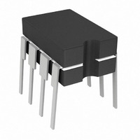
IC MOSFET DRIVER 6A HS 8CDIP
Manufacturer
Microchip Technology
Type
Microcontrollerr
Datasheet
1.TC429CPA.pdf
(18 pages)
Specifications of TC429MJA
Configuration
Low-Side
Input Type
Inverting
Delay Time
53ns
Current - Peak
6A
Number Of Configurations
1
Number Of Outputs
1
Voltage - Supply
7 V ~ 18 V
Operating Temperature
-55°C ~ 125°C
Mounting Type
Through Hole
Package / Case
8-CDIP (0.300", 7.62mm)
Rise Time
35 ns
Fall Time
35 ns
Supply Voltage (min)
7 V
Supply Current
12 mA
Maximum Power Dissipation
800 mW
Maximum Operating Temperature
+ 125 C
Mounting Style
Through Hole
Minimum Operating Temperature
- 55 C
Number Of Drivers
1
Lead Free Status / RoHS Status
Lead free / RoHS Compliant
High Side Voltage - Max (bootstrap)
-
Lead Free Status / Rohs Status
Lead free / RoHS Compliant
Available stocks
Company
Part Number
Manufacturer
Quantity
Price


3.0
The descriptions of the pins are listed in Table 3-1.
TABLE 3-1:
3.1
The V
and is rated for 7.0V to 18V with respect to the ground
pin. The V
a local ceramic capacitor. The value of the capacitor
should be chosen based on the capacitive load that is
being driven. A value of 1.0 µF is suggested.
3.2
The MOSFET driver input is a high-impedance,
TTL/CMOS compatible input. The input also has
300 mV of hysteresis between the high and low thresh-
olds that prevents output glitching even when the rise
and fall time of the input signal is very slow.
2003 Microchip Technology Inc.
Pin No.
DD
1
2
3
4
5
6
7
8
PIN DESCRIPTIONS
Supply Input (V
input is the bias supply for the MOSFET driver
Control Input (INPUT)
DD
input should be bypassed to ground with
OUTPUT
OUTPUT
Symbol
INPUT
GND
GND
PIN FUNCTION TABLE
V
V
NC
DD
DD
Supply input, 7V to 18V
Control input. TTL/CMOS compatible logic input
No connection
Ground
Ground
CMOS push-pull output, common to pin 7
CMOS push-pull output, common to pin 6
Supply input, 7V to 18V
DD
)
Description
3.3
The MOSFET driver output is a low-impedance, CMOS
push-pull style output, capable of driving a capacitive
load with 6.0A peak currents.
3.4
The ground pins are the return path for the bias current
and for the high peak currents that discharge the load
capacitor. The ground pins should be tied into a ground
plane or have very short traces to the bias supply
source return.
3.5
No connection.
CMOS Push-Pull Output
(OUTPUT)
Ground (GND)
No Connect (NC)
DS21416C-page 7
TC429
Related parts for TC429MJA
Image
Part Number
Description
Manufacturer
Datasheet
Request
R

Part Number:
Description:
CMOS Power MOSFET Driver
Manufacturer:
Microchip Technology
Datasheet:

Part Number:
Description:
Manufacturer:
Microchip Technology Inc.
Datasheet:
Part Number:
Description:
Manufacturer:
Microchip Technology Inc.
Datasheet:
Part Number:
Description:
Manufacturer:
Microchip Technology Inc.
Datasheet:
Part Number:
Description:
Manufacturer:
Microchip Technology Inc.
Datasheet:
Part Number:
Description:
Manufacturer:
Microchip Technology Inc.
Datasheet:
Part Number:
Description:
Manufacturer:
Microchip Technology Inc.
Datasheet:
Part Number:
Description:
Manufacturer:
Microchip Technology Inc.
Datasheet:
Part Number:
Description:
Manufacturer:
Microchip Technology Inc.
Datasheet: