TC429MJA Microchip Technology, TC429MJA Datasheet - Page 8
TC429MJA
Manufacturer Part Number
TC429MJA
Description
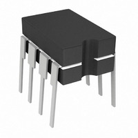
IC MOSFET DRIVER 6A HS 8CDIP
Manufacturer
Microchip Technology
Type
Microcontrollerr
Datasheet
1.TC429CPA.pdf
(18 pages)
Specifications of TC429MJA
Configuration
Low-Side
Input Type
Inverting
Delay Time
53ns
Current - Peak
6A
Number Of Configurations
1
Number Of Outputs
1
Voltage - Supply
7 V ~ 18 V
Operating Temperature
-55°C ~ 125°C
Mounting Type
Through Hole
Package / Case
8-CDIP (0.300", 7.62mm)
Rise Time
35 ns
Fall Time
35 ns
Supply Voltage (min)
7 V
Supply Current
12 mA
Maximum Power Dissipation
800 mW
Maximum Operating Temperature
+ 125 C
Mounting Style
Through Hole
Minimum Operating Temperature
- 55 C
Number Of Drivers
1
Lead Free Status / RoHS Status
Lead free / RoHS Compliant
High Side Voltage - Max (bootstrap)
-
Lead Free Status / Rohs Status
Lead free / RoHS Compliant
Available stocks
Company
Part Number
Manufacturer
Quantity
Price


TC429
4.0
4.1
Charging and discharging large capacitive loads
quickly requires large currents. For example, charging
a 2500 pF load to 18V in 25 nsec requires a 1.8A
current from the device's power supply.
To ensure low supply impedance over a wide frequency
range, a parallel capacitor combination is recom-
mended for supply bypassing. Low-inductance ceramic
disk capacitors with short lead lengths (< 0.5 in.)
should be used. A 1 µF film capacitor in parallel with
one or two 0.1 µF ceramic disk capacitors normally
provides adequate bypassing.
4.2
The high-current capability of the TC429 demands
careful PC board layout for best performance. Since
the TC429 is an inverting driver, any ground lead
impedance will appear as negative feedback that can
degrade switching speed. The feedback is especially
noticeable with slow rise-time inputs, such as those
produced by an open-collector output with resistor pull-
up. The TC429 input structure includes about 300 mV
of hysteresis to ensure clean transitions and freedom
from oscillation, but attention to layout is still
recommended.
Figure 4-3 shows the feedback effect in detail. As the
TC429 input begins to go positive, the output goes
negative and several amperes of current flow in the
ground lead. A PC trace resistance of as little as 0.05
can produce hundreds of millivolts at the TC429 ground
pins. If the driving logic is referenced to power ground,
the effective logic input level is reduced and oscillations
may result.
To ensure optimum device performance, separate
ground traces should be provided for the logic and
power connections. Connecting logic ground directly to
the TC429 GND pins ensures full logic drive to the input
and fast output switching. Both GND pins should be
connected to power ground.
DS21416C-page 8
APPLICATIONS INFORMATION
Supply Bypassing
Grounding
FIGURE 4-1:
Time Test Circuit.
FIGURE 4-2:
Output
Input
Input
18V
+5V
0V
0V
10%
2
5V
5V
90%
V
1, 8
t
TC429
OUTPUT
D1
DD
10%
OUTPUT
= 18V
INPUT
INPUT
TIME (100ns/DIV)
TIME (100ns/DIV)
4, 5
Inverting Driver Switching
Switching Speed.
t
F
2003 Microchip Technology Inc.
1 µF
6, 7
t
RISE
Input: 100 kHz,
square wave,
= t
C L = 2500pF
V
0.1 µF
C
t
C L = 2500pF
V
D2
S
FALL
S
L
90%
Output
= 7V
= 2500 pF
= 18V
100ns
100ns
t
10%
R
10 nsec
90%
Related parts for TC429MJA
Image
Part Number
Description
Manufacturer
Datasheet
Request
R

Part Number:
Description:
CMOS Power MOSFET Driver
Manufacturer:
Microchip Technology
Datasheet:

Part Number:
Description:
Manufacturer:
Microchip Technology Inc.
Datasheet:
Part Number:
Description:
Manufacturer:
Microchip Technology Inc.
Datasheet:
Part Number:
Description:
Manufacturer:
Microchip Technology Inc.
Datasheet:
Part Number:
Description:
Manufacturer:
Microchip Technology Inc.
Datasheet:
Part Number:
Description:
Manufacturer:
Microchip Technology Inc.
Datasheet:
Part Number:
Description:
Manufacturer:
Microchip Technology Inc.
Datasheet:
Part Number:
Description:
Manufacturer:
Microchip Technology Inc.
Datasheet:
Part Number:
Description:
Manufacturer:
Microchip Technology Inc.
Datasheet: