ISL6700IR Intersil, ISL6700IR Datasheet - Page 4
ISL6700IR
Manufacturer Part Number
ISL6700IR
Description
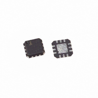
IC DRIVER HALF BRIDGE DUAL 12QFN
Manufacturer
Intersil
Datasheet
1.ISL6700IBZ.pdf
(8 pages)
Specifications of ISL6700IR
Configuration
Half Bridge
Input Type
PWM
Delay Time
70ns
Current - Peak
1.4A
Number Of Configurations
1
Number Of Outputs
2
High Side Voltage - Max (bootstrap)
80V
Voltage - Supply
9 V ~ 15 V
Operating Temperature
-40°C ~ 125°C
Mounting Type
Surface Mount
Package / Case
12-QFN
Lead Free Status / RoHS Status
Contains lead / RoHS non-compliant
Available stocks
Company
Part Number
Manufacturer
Quantity
Price


Absolute Maximum Ratings
Supply Voltage, V
LI and HI Voltages (Note 1) . . . . . . . . . . . . . . . . -0.3V to V
Voltage on HS (Note 1) . . . . . . . . . . . . . . . . . . . . . . . . . . 0V to 80V
Voltage on HB (Note 1) . . . . . . . . . . . . . . . . V
Voltage on LO (Note 1) . . . . . . . . . . . . . . . . . V
Voltage on HO (Note 1) . . . . . . . . . . . . . . . . V
Phase Slew Rate . . . . . . . . . . . . . . . . . . . . . . . . . . . . . . . . . . 20V/ns
Maximum Recommended Operating Conditions
Supply Voltage, V
Voltage on HS . . . . . . . . . . . . . . . . . . . . . . . . . . . . . . . . . . 0V to 75V
Voltage on HS (Note 2) . . . . . . . . . .(Repetitive Transient) -1V to 80V
Voltage on HB . . . . . . . . . . . . . . . . . . . . . . . . . . V
CAUTION: Stresses above those listed in “Absolute Maximum Ratings” may cause permanent damage to the device. This is a stress only rating and operation of the
device at these or any other conditions above those indicated in the recommended operating conditions of this specification is not implied.
NOTES:
Electrical Specifications
SUPPLY CURRENTS & UNDERVOLTAGE PROTECTION
V
V
V
HB Off Quiescent Current
HB On Quiescent Current
HB Operating Current
HB Operating Current
HS Leakage Current
V
V
Undervoltage Hysteresis
HB Undervoltage Threshold
INPUT PINS: LI and HI
Low Level Input Voltage
High Level Input Voltage
Input Voltage Hysteresis
Low Level Input Current
High Level Input Current
1. All voltages referenced to V
2. Based on V
3. θ
4. θ
DD
DD
DD
DD
DD
V
“case temp” is measured at the center of the exposed metal pad on the package underside. See Tech Brief TB379.
JA
JA
DD
Quiescent Current
Operating Current
Operating Current
Rising Undervoltage Threshold
Falling Undervoltage Threshold
is measured in free air with the component mounted on a high effective thermal conductivity test board with “direct attach” features. θ
is measured with the component mounted on a high effective thermal conductivity test board in free air. See Tech Brief TB379 for details.
+V
F
, where V
PARAMETERS
DD
DD
DD
=15V. The magnitude of the allowable negative transient on the HS pin is a function of the V
(Note 1) . . . . . . . . . . . . . . . . . . . -0.3V to 16V
. . . . . . . . . . . . . . . . . . . . . . . . . . . . . 9V to 15V
HS
is the magnitude of the allowable negative transient and V
SS
4
unless otherwise specified.
V
DD
= V
SYMBOL
V
HB
V
UVHYS
VHBUV
DDUV+
I
I
I
I
I
DDUV-
I
I
HS
HS
DDO
DDO
HBH
HBO
HBO
HS
I
HBL
HLK
V
V
I
DD
I
IH
= 12V, V
IL
SS
IH
IL
-0.3V to V
+7.5V to V
-0.3V to V
-0.3 to V
SS
LI = 0 or V
f = 50kHz
f = 500kHz
HI = 0
HI = V
f = 50kHz, C
f = 500kHz, C
V
V
Referenced to HS
Full Operating Conditions
Full Operating Conditions
V
V
HS
HB
IN
IN
DD
DD
HB
HS
HS
= V
= 0V, Full Operating Conditions
= 5V, Full Operating Conditions
= 80V
= 96V
+0.3V
+0.3V
+0.3V
+V
+V
DD
HS
DD
DD
TEST CONDITIONS
= 0V, No Load on LO or HO, Unless Otherwise Specified
DD
ISL6700
L
L
= 1000pF
= 1000pF
Thermal Information
Thermal Resistance (Typical)
Max Power Dissipation at 25°C in Free Air (SOIC, Note 3). 1.316W
Max Power Dissipation at 25°C in Free Air (QFN, Note 4) . .2.976W
Maximum Storage Temperature Range . . . . . . . . . .-65°C to +150°C
Maximum Junction Temperature Range . . . . . . . . .-40°C to +150°C
Maximum Lead Temperature (Soldering 10s) . . . . . . . . . . . +300°C
For Recommended soldering conditions see Tech Brief TB389.
SOIC (Note 3) . . . . . . . . . . . . . . . . . . .
QFN (Note 4) . . . . . . . . . . . . . . . . . . . .
(SOIC - Lead Tips Only)
F
is the forward voltage drop of the bootstrap diode.
0.17
MIN
-70
6.8
6.5
4.8
0.8
30
-
-
-
-
-
-
-
-
-
-
T
J
TYP
1.25
1.45
0.45
= 25°C
170
100
115
1.9
2.0
2.5
2.4
7.6
7.1
5.3
1.6
1.7
-60
-
DD
supply voltage. V
MAX
8.25
0.75
240
130
2.2
2.2
3.0
1.5
1.8
2.8
7.8
6.5
2.2
-30
1
-
-
θ
T
JA
6.25
0.15
MIN
J
6.5
4.0
0.8
-80
30
-
-
-
-
-
-
-
-
-
-
= -40°C TO
(°C/W)
95
49
125°C
MAX
December 29, 2004
0.90
250
145
-30
HS
2.4
2.5
4.0
1.8
2.0
3.0
8.5
8.1
7.5
2.2
1
-
-
<15.6V-
θ
JC
UNITS
N/A
FN9077.6
(°C/W)
JC
7
mA
mA
mA
mV
mA
mA
mA
µA
µA
µA
µA
V
V
V
V
V
V
, the
Related parts for ISL6700IR
Image
Part Number
Description
Manufacturer
Datasheet
Request
R

Part Number:
Description:
Intersil Corporation [CMOS Serial Controller Interface]
Manufacturer:
Intersil Corporation
Datasheet:
Part Number:
Description:
Manufacturer:
Intersil Corporation
Datasheet:
Part Number:
Description:
357-036-542-201 CARDEDGE 36POS DL .156 BLK LOPRO
Manufacturer:
Intersil Corporation
Datasheet:
Part Number:
Description:
1024-Word x 4-Bit LSI Static RAM
Manufacturer:
Intersil Corporation
Datasheet:
Part Number:
Description:
General Purpose NPN Transistor Arrays FN341.4
Manufacturer:
Intersil Corporation
Datasheet:
Part Number:
Description:
CMOS 16-Bit Microprocessor
Manufacturer:
Intersil Corporation
Datasheet:
Part Number:
Description:
Manufacturer:
Intersil Corporation
Datasheet:
Part Number:
Description:
Manufacturer:
Intersil Corporation
Datasheet:
Part Number:
Description:
Manufacturer:
Intersil Corporation
Datasheet:
Part Number:
Description:
Manufacturer:
Intersil Corporation
Datasheet:
Part Number:
Description:
CMOS 6-Bit Latch and Decoder Memory Interfaces
Manufacturer:
Intersil Corporation
Datasheet:
Part Number:
Description:
CA3046General Purpose NPN Transistor Arrays
Manufacturer:
Intersil Corporation
Datasheet:
Part Number:
Description:
Manufacturer:
Intersil Corporation
Datasheet:
Part Number:
Description:
TR909 DLC/FLC SLIC with Low Power Standby
Manufacturer:
Intersil Corporation
Datasheet:
Part Number:
Description:
Manufacturer:
Intersil Corporation
Datasheet: