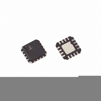
ISL6614CR Intersil, ISL6614CR Datasheet - Page 8

ISL6614CR
Manufacturer Part Number
ISL6614CR
Description
IC DRIVER MOSF DUAL SYNC 16QFN
Manufacturer
Intersil
Datasheet
1.ISL6614CBZ.pdf
(12 pages)
Specifications of ISL6614CR
Configuration
High and Low Side, Synchronous
Input Type
PWM
Delay Time
10.0ns
Current - Peak
1.25A
Number Of Configurations
2
Number Of Outputs
4
High Side Voltage - Max (bootstrap)
36V
Voltage - Supply
10.8 V ~ 13.2 V
Operating Temperature
0°C ~ 85°C
Mounting Type
Surface Mount
Package / Case
16-VQFN Exposed Pad, 16-HVQFN, 16-SQFN, 16-DHVQFN
Lead Free Status / RoHS Status
Contains lead / RoHS non-compliant
Available stocks
Company
Part Number
Manufacturer
Quantity
Price
Company:
Part Number:
ISL6614CRT
Manufacturer:
QPSM
Quantity:
7 089
Company:
Part Number:
ISL6614CRZ-T
Manufacturer:
INTERSIL/PB-FREE
Quantity:
11 994
Part Number:
ISL6614CRZ-T
Manufacturer:
INTERSIL
Quantity:
20 000
Description
Operation
Designed for versatility and speed, the ISL6614 MOSFET
driver controls both high-side and low-side N-Channel FETs
of two half-bridge power trains from two externally provided
PWM signals.
Prior to VCC exceeding its POR level, the Pre-POR
overvoltage protection function is activated; the upper gate
(UGATE) is held low and the lower gate (LGATE), controlled by
the Pre-POR overvoltage protection circuits, is connected to the
PHASE. Once the VCC voltage surpasses the VCC Rising
Threshold (See “Electrical Specifications” table on page 5), the
PWM signal takes control of gate transitions. A rising edge on
PWM initiates the turn-off of the lower MOSFET (see “TIMING
DIAGRAM” on page 8). After a short propagation delay [t
the lower gate begins to fall. Typical fall times [t
in the “Electrical Specifications” table on page 5. Adaptive
shoot-through circuitry monitors the PHASE voltage and
determines the upper gate delay time [t
both the lower and upper MOSFETs from conducting
simultaneously. Once this delay period is complete, the upper
gate drive begins to rise [t
A falling transition on PWM results in the turn-off of the upper
MOSFET and the turn-on of the lower MOSFET. A short
propagation delay [t
begins to fall [t
determines the lower gate delay time, t
voltage and the UGATE voltage are monitored, and the lower
gate is allowed to rise after PHASE drops below a level or the
voltage of UGATE to PHASE reaches a level depending upon
the current direction (See the following section for details). The
lower gate then rises [t
Advanced Adaptive Zero Shoot-Through Deadtime
Control (Patent Pending)
These drivers incorporate a unique adaptive deadtime control
technique to minimize deadtime, resulting in high efficiency
PWM
UGATE
LGATE
t
PDLL
FU
]. Again, the adaptive shoot-through circuitry
PDLU
RL
] is encountered before the upper gate
], turning on the lower MOSFET.
RU
] and the upper MOSFET turns on.
t
FL
8
t
PDHU
t
RU
PDHL
PDHU
t
PDHL
. The PHASE
]. This prevents
FL
] are provided
FIGURE 1. TIMING DIAGRAM
t
RL
t
PDLU
PDLL
t
FU
],
ISL6614
1.5V<PWM<3.2V
from the reduced freewheeling time of the lower MOSFETs’
body-diode conduction, and to prevent the upper and lower
MOSFETs from conducting simultaneously. This is
accomplished by ensuring either rising gate turns on its
MOSFET with minimum and sufficient delay after the other has
turned off.
During turn-off of the lower MOSFET, the PHASE voltage is
monitored until it reaches a -0.2V/+0.8V trip point for a
forward/reverse current, at which time the UGATE is released
to rise. An auto-zero comparator is used to correct the
r
detection of the -0.2V phase level during r
period. In the case of zero current, the UGATE is released
after 35ns delay of the LGATE dropping below 0.5V. During
the phase detection, the disturbance of LGATE’s falling
transition on the PHASE node is blanked out to prevent falsely
tripping. Once the PHASE is high, the advanced adaptive
shoot-through circuitry monitors the PHASE and UGATE
voltages during a PWM falling edge and the subsequent
UGATE turn-off. If either the UGATE falls to less than 1.75V
above the PHASE or the PHASE falls to less than +0.8V, the
LGATE is released to turn on.
Three-State PWM Input
A unique feature of these drivers and other Intersil drivers is
the addition of a shutdown window to the PWM input. If the
PWM signal enters and remains within the shutdown window
for a set holdoff time, the driver outputs are disabled and
both MOSFET gates are pulled and held low. The shutdown
state is removed when the PWM signal moves outside the
shutdown window. Otherwise, the PWM rising and falling
thresholds outlined in the “Electrical Specifications” table on
page 5 determine when the lower and upper gates are
enabled.
This feature helps prevent a negative transient on the output
voltage when the output is shut down, eliminating the
DS(ON)
t
TSSHD
drop in the phase voltage preventing from false
t
PDTS
t
1.0V<PWM<2.6V
TSSHD
DS(ON)
conduction
t
PDTS
May 5, 2008
FN9155.5


