HIP6602BCR Intersil, HIP6602BCR Datasheet
HIP6602BCR
Specifications of HIP6602BCR
Available stocks


Related parts for HIP6602BCR


HIP6602BCR Summary of contents
Page 1
... HIP6602BCRZ-T (Note 5x5 QFN Tape and Reel (Pb-Free) HIP6602BCRZA (Note HIP6602BCRZA-T (Note 5x5 QFN Tape and Reel (Pb-Free) NOTE: 1. Intersil Pb-free plus anneal products employ special Pb-free material sets; molding compounds/die attach materials and 100% matte tin plate termination finish, which are RoHS compliant and compatible with both SnPb and Pb-free soldering operations ...
Page 2
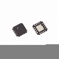
... PHASE2 8 SHOOT- THROUGH 10K PROTECTION 10K PGND CONTROL LOGIC PVCC 10K SHOOT- 10K THROUGH PROTECTION PGND For HIP6602BCR, the PAD on the bottom side of the PAD package MUST be soldered to the PC board HIP6602 (16 LD QFN) TOP VIEW GND 1 12 UG1 LG1 2 11 BOOT1 ...
Page 3
Typical Application - 2 Channel Converter Using a HIP6302 and a HIP6602B Gate Driver FB COMP V VSEN CC ISEN1 PGOOD PWM1 MAIN CONTROL HIP6302 VID PWM2 ISEN2 FS/DIS GND 3 HIP6602B +5V BOOT1 +12V UGATE1 VCC PHASE1 LGATE1 PWM1 ...
Page 4
Typical Application - 4 Channel Converter Using a HIP6303 and HIP6602B Gate Driver COMP FB V VSEN CC ISEN1 PWM1 PGOOD EN PWM2 ISEN2 MAIN CONTROL HIP6303 VID ISEN3 FS/DIS PWM3 PWM4 GND ISEN4 4 HIP6602B +12V BOOT1 UGATE1 VCC ...
Page 5
Absolute Maximum Ratings Supply Voltage (VCC .15V Supply ...
Page 6
Functional Pin Descriptions PWM1 (Pin 1) and PWM2 (Pin 2), (Pins 15 and 16 QFN) The PWM signal is the control input for the driver. The PWM signal can enter three distinct states during operation, see the three-state PWM Input ...
Page 7
A falling transition on PWM indicates the turn-off of the upper MOSFET and the turn-on of the lower MOSFET. A short propagation delay [TPDL UGATE before the upper gate begins to fall [TF adaptive shoot-through circuitry determines the lower gate ...
Page 8
MOSFETs. The total chip power dissipation is approximated as 1. PVCC ...
Page 9
Typical Performance Curves 1200 5nF 1000 4nF = 3nF 800 600 2nF U L 400 1nF ...
Page 10
Typical Performance Curves FIGURE 8. POWER DISSIPATION vs LOADING, PVCC = 5V 10 HIP6602B (Continued) 600 PVCC = 5V, VCC = 12V 500 1.5MHz 2MHz 1MHz 400 300 500kHz 200 200kHz 100 GATE CAPACITANCE (C U ...
Page 11
... Dimensions D2 and E2 are for the exposed pads which provide improved electrical and thermal performance. 8. Nominal dimensions are provided to assist with PCB Land Pattern Design efforts, see Intersil Technical Brief TB389. 9. Features and dimensions A2, A3, D1, E1, P & θ are present when Anvil singulation method is used and not present for saw singulation ...
Page 12
... Accordingly, the reader is cautioned to verify that data sheets are current before placing orders. Information furnished by Intersil is believed to be accurate and reliable. However, no responsibility is assumed by Intersil or its subsidiaries for its use; nor for any infringements of patents or other rights of third parties which may result from its use ...