EL7156CSZ-T7 Intersil, EL7156CSZ-T7 Datasheet
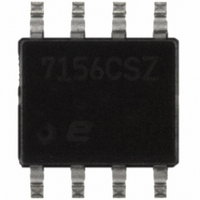
IC PIN DRIVER 3STATE 8-SOIC

EL7156CSZ-T7

Manufacturer Part Number
EL7156CSZ-T7
Description
IC PIN DRIVER 3STATE 8-SOIC
Manufacturer
Intersil
Type
High Sider
Datasheet

Specifications of EL7156CSZ-T7

Configuration
High or Low Side
Input Type
Non-Inverting
Delay Time
10ns
Current - Peak
3.5A
Number Of Configurations
1
Number Of Outputs
1
Voltage - Supply
4.5 V ~ 16.5 V
Operating Temperature
-40°C ~ 85°C
Mounting Type
Surface Mount
Package / Case
8-SOIC (3.9mm Width)
Current - Output / Channel
200mA
On-state Resistance
2.7 Ohm
Current - Peak Output
3.5A
Peak Reflow Compatible (260 C)
Yes
Rohs Compliant
Yes
Lead Free Status / RoHS Status
Lead free / RoHS Compliant
Other names
EL7156CSZ-T7TR

Available stocks

Company
Part Number
Manufacturer
Quantity
Price
Part Number:
EL7156CSZ-T7
Manufacturer:
INTERSIL
Quantity:
3 000
Part Number:
EL7156CSZ-T7
Manufacturer:
Intersil
Quantity:
1 000
Part Number:
EL7156CSZ-T7
Manufacturer:
INTERSIL
Quantity:
20 000
High Performance Pin Driver
The EL7156 high performance pin driver with three-state is
suited to many ATE and level-shifting applications. The 3.5A
peak drive capability makes this part an excellent choice
when driving high capacitance loads.
The output pin OUT is connected to input pins VH or VL
respectively, depending on the status of the IN pin. When the
OE pin is active low, the output is placed in the three-state
mode. The isolation of the output FETs from the power
supplies enables VH and VL to be set independently,
enabling level-shifting to be implemented. Related to the
EL7155, the EL7156 adds a lower supply pin VS- and makes
VL an isolated and independent input. This feature adds
applications flexibility and improves switching response due
to the increased enhancement of the output FETs.
This pin driver has improved performance over existing pin
drivers. It is specifically designed to operate at voltages
down to 0V across the switch elements while maintaining
good speed and ON-resistance characteristics.
Available in the 8 Ld SOIC and 8 Ld PDIP packages, the
EL7156 is specified for operation over the full -40°C to
+85°C temperature range.
Pinout
GND
VS+
OE
IN
1
2
3
4
(8 LD PDIP, SOIC)
TOP VIEW
O
G
C
L
I
EL7156
®
1
Data Sheet
8
7
6
5
VH
OUT
VL
VS-
1-888-INTERSIL or 1-888-468-3774
CAUTION: These devices are sensitive to electrostatic discharge; follow proper IC Handling Procedures.
Features
• Clocking speeds up to 40MHz
• 15ns t
• 0.5ns rise and fall times mismatch
• 0.5ns t
• 3.5pF typical input capacitance
• 3.5A peak drive
• Low ON-resistance of 3.5Ω
• High capacitive drive capability
• Operates from 4.5V to 16.5V
• Pb-free plus anneal available (RoHS compliant)
Applications
• ATE/burn-in testers
• Level shifting
• IGBT drivers
• CCD drivers
Ordering Information
NOTE: Intersil Pb-free plus anneal products employ special Pb-free
material sets; molding compounds/die attach materials and 100%
matte tin plate termination finish, which are RoHS compliant and
compatible with both SnPb and Pb-free soldering operations. Intersil
Pb-free products are MSL classified at Pb-free peak reflow
temperatures that meet or exceed the Pb-free requirements of
IPC/JEDEC J STD-020.
*Pb-free PDIPs can be used for through hole wave solder processing
only. They are not intended for use in Reflow solder processing
applications.
EL7156CN
EL7156CNZ
(Note)
EL7156CS
EL7156CS-T7
EL7156CS-T13
EL7156CSZ
(Note)
EL7156CSZ-T7
(Note)
EL7156CSZ-T13
(Note)
PART NUMBER
All other trademarks mentioned are the property of their respective owners.
R
ON
Copyright © Intersil Americas Inc. 2003, 2005, 2007. All Rights Reserved.
/t
|
F
May 2, 2007
-t
Intersil (and design) is a registered trademark of Intersil Americas Inc.
at 2000pF C
OFF
EL7156CN
EL7156CN Z
7156CS
7156CS
7156CS
7156CSZ
7156CSZ
7156CSZ
prop delay mismatch
MARKING
PART
LOAD
TAPE &
REEL
13”
13”
7”
7”
-
-
-
-
8 Ld PDIP
8 Ld PDIP*
(Pb-free)
8 Ld SOIC
8 Ld SOIC
8 Ld SOIC
8 Ld SOIC
(Pb-free)
8 Ld SOIC
(Pb-free)
8 Ld SOIC
(Pb-free)
PACKAGE
EL7156
FN7280.3
MDP0031
MDP0031
MDP0027
MDP0027
MDP0027
MDP0027
MDP0027
MDP0027
DWG. #
PKG.

Related parts for EL7156CSZ-T7

EL7156CSZ-T7 Summary of contents

Page 1

... VL EL7156CS-T13 EL7156CSZ 5 VS- (Note) EL7156CSZ-T7 (Note) EL7156CSZ-T13 (Note) NOTE: Intersil Pb-free plus anneal products employ special Pb-free material sets; molding compounds/die attach materials and 100% matte tin plate termination finish, which are RoHS compliant and compatible with both SnPb and Pb-free soldering operations. Intersil ...

Page 2

... Ambient Operating Temperature . . . . . . . . . . . . . . . .-40°C to +85°C - -0.3V, V +0.3V Operating Junction Temperature . . . . . . . . . . . . . . . . . . . . . . +125° Power Dissipation . . . . . . . . . . . . . . . . . . . . . . . . . . . . . . see curves Pb-free reflow profile . . . . . . . . . . . . . . . . . . . . . . . . . .see link below http://www.intersil.com/pbfree/Pb-FreeReflow.asp *Pb-free PDIPs can be used for through hole wave solder processing only. They are not intended for use in Reflow solder processing applications ...

Page 3

Electrical Specifications +5V PARAMETER DESCRIPTION INPUT V Logic ‘1’ Input Voltage IH I Logic ‘1’ Input Current IH V Logic ‘0’ Input Voltage IL I Logic ‘0’ Input Current IL C Input Capacitance IN R ...

Page 4

Typical Performance Curves JEDEC JESD51-3 LOW EFFECTIVE THERMAL CONDUCTIVITY TEST BOARD 1.0 PDIP8 θ = 100°C/W JA 0.8 0.6 SOIC8 0.4 θ = 160°C AMBIENT TEMPERATURE (°C) FIGURE 1. PACKAGE POWER DISSIPATION ...

Page 5

Typical Performance Curves C = 2000pF +25° d d SUPPLY VOLTAGE (V) FIGURE 7. PROPAGATION DELAY vs SUPPLY VOLTAGE +15V +25° ...

Page 6

Truth Table Timing Diagram INVERTED Standard Test Configuration 4.7µ 10kΩ 6 EL7156 Operating Voltage Range OUT Three-state V Three-state ...

Page 7

Pin Descriptions PIN NAME 1 VS+ Positive Supply Voltage 2 OE Output Enable 3 IN Input 4 GND Ground 5 VS- Negative Supply Voltage 6 VL Lower Output Voltage 7 OUT Output 8 VH High Output Voltage Block Diagram V ...

Page 8

Applications Information Product Description The EL7156 is a high performance 40MHz pin driver. It contains two analog switches connecting VH and VL to OUT. Depending on the value of the IN pin, one of the two switches will be closed ...

Page 9

... Accordingly, the reader is cautioned to verify that data sheets are current before placing orders. Information furnished by Intersil is believed to be accurate and reliable. However, no responsibility is assumed by Intersil or its subsidiaries for its use; nor for any infringements of patents or other rights of third parties which may result from its use ...

Page 10

Small Outline Package Family (SO PIN #1 I.D. MARK 0.010 SEATING PLANE 0.004 C 0.010 MDP0027 SMALL OUTLINE PACKAGE FAMILY (SO) SYMBOL SO-8 SO-14 ...

Related keywords