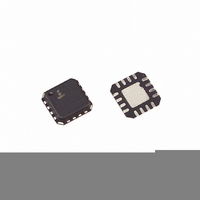
EL7457CLZ Intersil, EL7457CLZ Datasheet - Page 9

EL7457CLZ
Manufacturer Part Number
EL7457CLZ
Description
IC DRIVER CMOS QUAD 40MHZ 16QFN
Manufacturer
Intersil
Type
High Side/Low Side Driverr
Datasheet
1.EL7457CSZ-T7.pdf
(12 pages)
Specifications of EL7457CLZ
Configuration
High or Low Side
Input Type
Non-Inverting
Delay Time
14.5ns
Current - Peak
2A
Number Of Configurations
1
Number Of Outputs
4
Voltage - Supply
4.5 V ~ 18 V
Operating Temperature
-40°C ~ 85°C
Mounting Type
Surface Mount
Package / Case
16-VQFN Exposed Pad, 16-HVQFN, 16-SQFN, 16-DHVQFN
Current - Output / Channel
100mA
On-state Resistance
3 Ohm
Current - Peak Output
2A
Lead Free Status / RoHS Status
Lead free / RoHS Compliant
Available stocks
Company
Part Number
Manufacturer
Quantity
Price
Company:
Part Number:
EL7457CLZ
Manufacturer:
INTERSIL
Quantity:
1 815
Part Number:
EL7457CLZ
Manufacturer:
INTERSIL
Quantity:
20 000
Company:
Part Number:
EL7457CLZ-T7
Manufacturer:
Intersil
Quantity:
13 000
Part Number:
EL7457CLZ-T7
Manufacturer:
INTERSIL
Quantity:
20 000
Block Diagram
Applications Information
Product Description
The EL7457 is a high performance 40MHz high speed quad
driver. Each channel of the EL7457 consists of a single P-
channel high side driver and a single N-channel low side
driver. These 3Ω devices will pull the output (OUT
the high or low voltage, on V
depending on the input logic signal (IN
that there is only one set of high and low voltage pins.
A common output enable (OE) pin is available on the
EL7457. This pin, when pulled low will put all outputs in to
the high impedance state.
The EL7457 is available in 16-pin SO (0.150"), 16-pin
QSOP, and ultra-small 16-pin QFN packages. The relevant
package should be chosen depending on the calculated
power dissipation.
Supply Voltage Range and Input Compatibility
The EL7457 is designed for operation on supplies from 5V to
15V with 10% tolerance (i.e. 4.5V to 18V). The table on page
6 shows the specifications for the relationship between the
V
contain a true analog switch and therefore V
be less than V
All input pins are compatible with both 3V and 5V CMOS
signals With a positive supply (V
also compatible with TTL inputs.
Power Supply Bypassing
When using the EL7457, it is very important to use adequate
power supply bypassing. The high switching currents
developed by the EL7457 necessitate the use of a bypass
capacitor on both the positive and negative supplies. It is
recommended that a 4.7µF tantalum capacitor be used in
parallel with a 0.1µF low-inductance ceramic MLC capacitor.
These should be placed as close to the supply pins as
possible. It is also recommended that the V
have some level of bypassing, especially if the EL7457 is
driving highly capacitive loads.
S
+, V
S
-, V
H
, V
H
.
L
, and GND pins. The EL7457 does not
H
9
and V
INPUT
GND
S
V
V
+) of 5V, the EL7457 is
S
S
+
-
L
respectively,
X
). It should be noted
SHIFTER
H
LEVEL
L
and V
should always
X
) to either
L
pins
EL7457
OE
CONTROL
3-STATE
Power Dissipation Calculation
When switching at high speeds, or driving heavy loads, the
EL7457 drive capability is limited by the rise in die
temperature brought about by internal power dissipation. For
reliable operation die temperature must be kept below
T
dissipation for a given application prior to selecting package
type.
Power dissipation may be calculated:
PD
where:
Having obtained the application’s power dissipation, the
maximum junction temperature can be calculated:
T
where:
JMAX
JMAX
V
V
V
C
C
I
f is frequency
T
T
PD is the power dissipation calculated above
θ
application (package + PCB combination). Refer to the
Package Power Dissipation curves on page 6.
S
JA
S
S
OUT
JMAX
MAX
L
INT
=
is the quiescent supply current (3mA max)
-)
is the load capacitance
is the total power supply to the EL7457 (from V
(
is the thermal resistance, junction to ambient, of the
V
(125°C). It is necessary to calculate the power
=
is the internal load capacitance (80pF max)
S
is the swing on the output (V
is the maximum ambient operating temperature
T
is the maximum junction temperature (125°C)
×
MAX
I
V
V
S
H
L
)
+
+
∑
4
1
Θ
JA
OUTPUT
(
C
INT
×
PD
×
V
2
S
×
f
)
+
(
C
L
H
×
- V
V
2
OUT
L
)
×
f
)
January 3, 2005
S
FN7288.3
+ to


