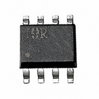
IPS521G International Rectifier, IPS521G Datasheet - Page 2

IPS521G
Manufacturer Part Number
IPS521G
Description
IC MOSFET HS PWR SW 5A 8-SOIC
Manufacturer
International Rectifier
Type
High Sider
Datasheet
1.IPS521G.pdf
(9 pages)
Specifications of IPS521G
Input Type
Non-Inverting
Number Of Outputs
1
On-state Resistance
80 mOhm
Current - Output / Channel
1.6A
Current - Peak Output
10A
Voltage - Supply
5.5 V ~ 35 V
Operating Temperature
-40°C ~ 150°C
Mounting Type
Surface Mount
Package / Case
8-SOIC (3.9mm Width)
Current, Leakage, Offset
50 mA
Current, Supply
1.6 A
Package Type
SOIC-8
Polarization
N-Channel
Power Dissipation
1 W
Resistance, Drain To Source On
100 Milliohms
Temperature, Operating, Maximum
+150 °C
Temperature, Operating, Minimum
–40 °C
Thermal Resistance, Junction To Ambient
125 °C/W
Time, Turn-off Delay
35 ms
Time, Turn-on Delay
10 ms
Voltage, Input
7 V
Voltage, Input, High Level
5.5 V
Voltage, Input, Low Level
0.9 V
Voltage, Supply
65 V
Lead Free Status / RoHS Status
Contains lead / RoHS non-compliant
Other names
*IPS521G
Available stocks
Company
Part Number
Manufacturer
Quantity
Price
Part Number:
IPS521G
Manufacturer:
IR
Quantity:
20 000
Company:
Part Number:
IPS521GTR
Manufacturer:
AMIS
Quantity:
34
Part Number:
IPS521GTRBPF
Manufacturer:
IR
Quantity:
20 000
Company:
Part Number:
IPS521GTRPBF
Manufacturer:
IR
Quantity:
13 000
IPS521G
Thermal Characteristics
Recommended Operating Conditions
These values are given for a quick design. For operation outside these conditions, please consult the application notes.
(1) Limited by junction temperature (pulsed current limited also by internal wiring)
Absolute Maximum Ratings
Absolute maximum ratings indicate sustained limits beyond which damage to the device may occur. All voltage parameters
are referenced to GROUND lead. (T j = 25
Symbol Parameter
R th1
R th2
Symbol Parameter
V cc
V IH
V IL
I out
R in
R dg
Symbol Parameter
V out
V offset
V in
I in, max
V dg
I dg, max
I sd
I sd
ESD1
ESD2
P d
T j max.
Vcc max.
Tc=85
2
cont.
pulsed
o
C
Thermal resistance with standard footprint
Thermal resistance with 1" square footprint
Continuous V cc voltage
High level input voltage
Low level input voltage
Continuous output current
Recommended resistor in series with IN pin
Recommended resistor in series with DG pin
Maximum output voltage
Maximum logic ground to load ground offset V cc -50
Maximum Input voltage
Maximum positive IN current
Maximum diagnostic output voltage
Maximum diagnostic output current
Diode max. permanent current
Diode max. pulsed current
Electrostatic discharge voltage
Electrostatic discharge voltage
Maximum power dissipation
Max. storage & operating junction temp.
Maximum Vcc voltage
( TAmbient = 85
(rth = 125
(rth=125
o
C, Tj = 125
(1)
(1)
o
(Machine Model)
C/W)
o
(Human Body)
o
(1)
C/W)
C unless otherwise specified).
o
C, R th = 100
V cc -50
Min.
Min.
-0.3
-0.3
-40
—
—
—
—
—
—
-5
-1
—
—
o
C/W)
V cc +0.3
V cc +0.3
Typ.
Max.
+150
5.5
5.5
1.4
0.5
10
10
10
50
4
1
Max. Units Test Conditions
Units
mA
mA
o
W
V
V
A
kV
C
V
o
C/W
C=100pF, R=1500
C=200pF, R=0
-0.3
8 Lead SOIC
Min.
5.5
—
4
10
Test Conditions
4
Max.
5.5
0.9
1.6
35
6
20
L=10 H
www.irf.com
Units
k
A
V


