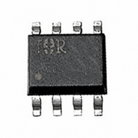
IPS521G International Rectifier, IPS521G Datasheet - Page 3

IPS521G
Manufacturer Part Number
IPS521G
Description
IC MOSFET HS PWR SW 5A 8-SOIC
Manufacturer
International Rectifier
Type
High Sider
Datasheet
1.IPS521G.pdf
(9 pages)
Specifications of IPS521G
Input Type
Non-Inverting
Number Of Outputs
1
On-state Resistance
80 mOhm
Current - Output / Channel
1.6A
Current - Peak Output
10A
Voltage - Supply
5.5 V ~ 35 V
Operating Temperature
-40°C ~ 150°C
Mounting Type
Surface Mount
Package / Case
8-SOIC (3.9mm Width)
Current, Leakage, Offset
50 mA
Current, Supply
1.6 A
Package Type
SOIC-8
Polarization
N-Channel
Power Dissipation
1 W
Resistance, Drain To Source On
100 Milliohms
Temperature, Operating, Maximum
+150 °C
Temperature, Operating, Minimum
–40 °C
Thermal Resistance, Junction To Ambient
125 °C/W
Time, Turn-off Delay
35 ms
Time, Turn-on Delay
10 ms
Voltage, Input
7 V
Voltage, Input, High Level
5.5 V
Voltage, Input, Low Level
0.9 V
Voltage, Supply
65 V
Lead Free Status / RoHS Status
Contains lead / RoHS non-compliant
Other names
*IPS521G
Available stocks
Company
Part Number
Manufacturer
Quantity
Price
Part Number:
IPS521G
Manufacturer:
IR
Quantity:
20 000
Company:
Part Number:
IPS521GTR
Manufacturer:
AMIS
Quantity:
34
Part Number:
IPS521GTRBPF
Manufacturer:
IR
Quantity:
20 000
Company:
Part Number:
IPS521GTRPBF
Manufacturer:
IR
Quantity:
13 000
www.irf.com
Static Electrical Characteristics
(T j = 25
Switching Electrical Characteristics
V cc = 14V, Resistive Load = 2.8 , T
Symbol Parameter
Td off
E off
T diag
Td on
T r1
T r2
d V/dt (on) Turn ON d V/dt
E on
T f
d V/dt (off) Turn OFF d V/dt
Symbol Parameter
R ds(on)
@Tj=25
R ds(on)
(V cc =6V)
R ds(on)
@Tj=150
V cc oper. Operating voltage range
V
V
V f
I cc off
I cc on
I cc ac
V dgl
I oh
I ol
Idg
leakage
V ih
V il
I in , on
In hyst.
clamp 1
clamp 2
o
o
C, V cc = 14V unless otherwise specified.)
o
C
C
Turn-on delay time
Rise time to V out = V cc - 5V
Rise time V cc - 5V to V out = 90% of V cc
Turn ON energy
Turn-off delay time
Fall time to V out = 10% of V cc
Turn OFF energy
V out to V diag propagation delay
ON state resistance T j = 25
ON state resistance @ V cc = 6V
ON state resistance Tj = 150
V cc to OUT clamp voltage 1
V cc to OUT clamp voltage 2
Body diode forward voltage
Supply current when OFF
Supply current when ON
Ripple current when ON (AC RMS)
Low level diagnostic output voltage
Output leakage current
Output leakage current
Diagnostic output leakage current
IN high threshold voltage
IN low threshold voltage
On state IN positive current
Input hysteresis
j
= 25
o
o
C
C
o
C, (unless otherwise specified).
Min.
Min.
5.5
0.1
50
—
—
—
—
—
—
—
—
—
—
—
—
—
—
—
—
—
—
—
0
1
Typ. Max. Units Test Conditions
1500
Typ.
0.25
130
250
125
0.7
0.9
0.9
0.6
0.4
2.2
1.9
10
25
35
16
80
80
55
56
13
20
50
70
—
—
—
5
Max. Units Test Conditions
100
100
160
120
200
200
1.2
0.5
70
15
35
65
50
25
10
40
60
—
50
—
—
—
—
—
2
3
2
3
V/ s
V/ s
mA
m
V
V
V
V
A
A
A
J
J
s
s
s
A
I d = I sd
See figure 3
See figure 4
See figure 6
V in = 5V, I out = 5A
I d = 10mA
I d = 2.5A, V in = 0V
V in = 0V, V out = 0V
V in = 5V
V in = 5V
I dg = 1.6 mA
V out = 6V
V out = 0V
Vdg = 5.5V
V in = 5V
V in = 5V, I out = 5A
V in = 5V, I out = 2.5A
(see Fig.1 & 2)
IPS521G
(see Fig.1 & 2)
3


