IRSF3010S International Rectifier, IRSF3010S Datasheet
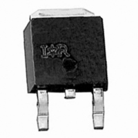
IC FET SMART SW 50V 11A D2PAK

IRSF3010S

Manufacturer Part Number
IRSF3010S
Description
IC FET SMART SW 50V 11A D2PAK
Manufacturer
International Rectifier
Type
High Side/Low Side Driverr
Datasheet

Specifications of IRSF3010S

Input Type
Non-Inverting
Number Of Outputs
1
On-state Resistance
70 mOhm
Current - Output / Channel
14A
Current - Peak Output
20A
Voltage - Supply
1.5 V ~ 10 V
Operating Temperature
-55°C ~ 155°C
Mounting Type
Surface Mount
Package / Case
D²Pak, TO-263 (2 leads + tab)
Lead Free Status / RoHS Status
Contains lead / RoHS non-compliant
Other names
*IRSF3010S

Available stocks

Company
Part Number
Manufacturer
Quantity
Price
Part Number:
IRSF3010S
Manufacturer:
IR
Quantity:
20 000
FULLY PROTECTED POWER MOSFET SWITCH
General Description:
The IRSF3010 is a three terminal monolithic
SMART POWER MOSFET with built in short cir-
cuit, over-temperature, ESD and over-voltage pro-
tections.
The on chip protection circuit latches off the
POWER MOSFET in case the drain current ex-
ceeds 14A (typical) or the junction temperature ex-
ceeds 165°C (typical) and keeps it off until the
input is driven low. The drain to source voltage
is actively clamped at 55V (typical), prior to the
avalanche of POWER MOSFET, thus improving
its performance during turn off with inductive
loads.
The input current requirements are very low
(300uA) which makes the IRSF3010 compatible with
most existing designs based on standard
POWER MOSFETs.
Applications:
DC Motor Drive
Solenoid Driver
Source
Drain
Features:
Rating Summary:
Extremely Rugged for Harsh Operating
Environments
Over Temperature Protection
Over Current Protection
Active Drain to Source Clamp
ESD Protection
Compatible with standard POWER
MOSFET
Low Operating Input Current
Monolithic Construction
Dual set/reset Threshold Input
Tab
V
R
I
T
E
Provisional Data Sheet No.PD-6.0027A
ds(sd)
IRSF3010
j(sd)
ds(clamp)
AS
ds(on)
IRSF3010S
1
2
3
Pin Assignment
Pin 1 - Input
Pin 2 - Drain
Pin 3 - Source
Tab - Drain
400 mJ
80 m
155 °C
11 A
50 V

Related parts for IRSF3010S

IRSF3010S Summary of contents

Page 1

... Over Current Protection Active Drain to Source Clamp ESD Protection Compatible with standard POWER MOSFET Low Operating Input Current Monolithic Construction Dual set/reset Threshold Input Drain Tab IRSF3010 IRSF3010S Source 155 °C 400 mJ Pin Assignment Pin 1 - Input Pin 2 - Drain Pin 3 - Source Tab - Drain ...

Page 2

Absolute Maximum Ratings Absolute Maximum Ratings indicate sustained limits beyond which damage to the device may occur 25°C unless otherwise specified.) Symbol V ds, max Continuous Drain to Source Voltage V in, max Continuous Input Voltage I ...

Page 3

Switching Electrical Characteristics 14V, Resistive Load °C.) Please refer to Figure 15 for switching time definitions. Symbol Parameter Definition t don Turn-On Delay time t r Rise Time ...

Page 4

T = 25°C 110 100 Vin = Vin = 5V 70 Vin = Ids (A) Fig Resistance vs Drain to Source Current 17 T ...

Page 5

Rise Time 1.00 On Delay 0.50 0. Input Voltage (Volts characteristics vs Input Voltag e 0 25°C 0.8 Off Delay 0.7 0.6 ...

Page 6

90% 10 don r Fig Definition of Switching times > t < t reset ds(sd Fig Definition ...

Page 7

7 ...

Page 8

8 ...

Page 9

9 ...

Page 10

Application Information Introduction Protected monolithic POWER MOSFETs offer simple, cost effective solutions in applications where extreme operating conditions can occur. The margin between the operating conditions and the absolute maxi- mum values can be narrowed resulting in better utilization of ...

Page 11

The typical waveforms at 7V input voltage are shown in figure 22. In typical switching applications, below 40kHz, the difference in switching losses between the IRSF3010 and the same size standard MOSFET is negligible. Input voltage 5V/ Drain voltage 5V/ ...

Related keywords