VNQ860SP STMicroelectronics, VNQ860SP Datasheet - Page 3
VNQ860SP
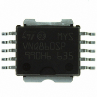
Manufacturer Part Number
VNQ860SP
Description
IC DRIVER 4CHAN HISIDE 10PWRSOIC
Manufacturer
STMicroelectronics
Type
High Sider
Datasheet
1.VNQ860.pdf
(13 pages)
Specifications of VNQ860SP
Input Type
Non-Inverting
Number Of Outputs
4
On-state Resistance
270 mOhm
Current - Output / Channel
250mA
Current - Peak Output
700mA
Voltage - Supply
5.5 V ~ 36 V
Operating Temperature
-40°C ~ 150°C
Mounting Type
Surface Mount
Package / Case
PowerSO-10 Exposed Bottom Pad
Supply Voltage (min)
5.5 V
Supply Current
120 mA
Maximum Power Dissipation
90000 mW
Maximum Operating Temperature
+ 150 C
Mounting Style
SMD/SMT
Minimum Operating Temperature
- 55 C
Lead Free Status / RoHS Status
Lead free / RoHS Compliant
Other names
497-4502-5
Available stocks
Company
Part Number
Manufacturer
Quantity
Price

Part Number:
VNQ860SP
Manufacturer:
ST
Quantity:
20 000
Company:
Part Number:
VNQ860SP-E
Manufacturer:
DYNEX
Quantity:
50
Company:
Part Number:
VNQ860SPTR-E
Manufacturer:
ST
Quantity:
3 492


THERMAL DATA
(1)
(2)
ELECTRICAL CHARACTERISTICS (8V<V
POWER
SWITCHING (V
PROTECTIONS (Per channel)
(dV
(dV
When mounted on FR4 printed circuit board with 0.5cm
When mounted on FR4 printed circuit board with 6cm
Symbol
Symbol
Symbol
R
I
I
Symbol
R
V
R
OUTleak
OUTleak
I
T
V
OUT
OUT
I
t
t
T
thj-case
thj-amb
R
LGND
V
V
demag
D(on)
D(off)
L(off)
thj-pin
(hyst)
I
T
USD
TSD
I
lim
CC
OV
ON
S
R
/dt)
/dt)
on
off
Operating supply voltage
Undervoltage shut-down
Overvoltage shut-down
On state resistance
(per channel)
Supply current
Output current
Off state output current
Off state output leakage
current
Off state output leakage
current
Current limitation
Thermal hysteresis
Thermal shut-down
temperature
Reset temperature
Turn-off output clamp voltage I
Thermal resistance junction-pins
Thermal resistance junction-ambient
Thermal resistance junction-case
Turn-on delay time
Turn-off delay time
Turn-on voltage slope
Turn-off voltage slope
CC
=24V) (Per channel)
Parameter
Parameter
Parameter
Parameter
I
I
Off state;
On state (all channels on)
V
V
V
V
T
V
V
R
V
R
V
R
R
OUT
OUT
OUT
CC
OUT
IN
IN
amb
IN
OUT
2
OUT
OUT
L
L
L
L
=96
=96
=96
=96
of copper area (at least 35 thick) connected to all V
2
CC
=V
=V
=V
-V
=0.25A; T
=0.25A
of copper area (at least 35 thick) connected to all V
=0.25A
=25
=0V
=10V; T
=21.6V
<36V; -40
OUT
GND
GND
=2.4V
STAT
Test Conditions
o
Test Conditions
Test Conditions
from V
from V
from V
from V
V
C
=0V
=0V; V
=0V; V
=V
CC
amb
IN
j
=24V; T
=25
=V
IN
IN
OUT
OUT
=25
CC
CC
o
C<T
rising edge to
falling edge to
GND
o
C
=V
=24V;
=2.4V to 19.2V
=21.6V to 2.4V
(MAX)
(MAX)
(MAX)
o
C
c
=24V
OUT
j
=25
<150
=24V;
o
C
o
C; unless otherwise specified)
SO-20
58
8
-
V
Min
0.35
CC
Min
Min
150
135
5.5
36
3
0
7
-47 V
Value
VNQ860 / VNQ860SP
Typ
0.75
0.25
CC
Typ
PowerSO-10
CC
Typ
175
0.7
42
70
10
40
15
4
5
CC
-52 V
pins.
52
37
pins.
1.4
-
(1)
(2)
Max
Max
CC
270
540
120
240
100
Max
200
5.5
1.1
36
48
10
10
1
-59
o
o
o
o
Unit
V s
V s
Unit
Unit
Unit
m
m
mA
mA
C/W
C/W
C/W
C/W
o
o
o
V
V
V
A
V
C
C
C
A
A
A
A
s
s
3/13
1
Related parts for VNQ860SP
Image
Part Number
Description
Manufacturer
Datasheet
Request
R

Part Number:
Description:
IC DRIVER HISIDE QUAD 20-SOIC
Manufacturer:
STMicroelectronics
Datasheet:

Part Number:
Description:
Quad channel high side driver
Manufacturer:
STMICROELECTRONICS [STMicroelectronics]
Datasheet:
Part Number:
Description:
IC DRIVER QUAD 36V 0.25A 20-SOIC
Manufacturer:
STMicroelectronics
Datasheet:

Part Number:
Description:
STMicroelectronics [RIPPLE-CARRY BINARY COUNTER/DIVIDERS]
Manufacturer:
STMicroelectronics
Datasheet:
Part Number:
Description:
STMicroelectronics [LIQUID-CRYSTAL DISPLAY DRIVERS]
Manufacturer:
STMicroelectronics
Datasheet:

Part Number:
Description:
BOARD EVAL FOR MEMS SENSORS
Manufacturer:
STMicroelectronics
Datasheet:
Part Number:
Description:
NPN TRANSISTOR POWER MODULE
Manufacturer:
STMicroelectronics
Datasheet:
Part Number:
Description:
TURBOSWITCH ULTRA-FAST HIGH VOLTAGE DIODE
Manufacturer:
STMicroelectronics
Datasheet:
Part Number:
Description:
Manufacturer:
STMicroelectronics
Datasheet:
Part Number:
Description:
DIODE / SCR MODULE
Manufacturer:
STMicroelectronics
Datasheet:
Part Number:
Description:
DIODE / SCR MODULE
Manufacturer:
STMicroelectronics
Datasheet:
Part Number:
Description:
Search -----> STE16N100
Manufacturer:
STMicroelectronics
Datasheet: