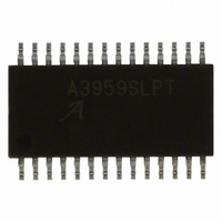
A3959SLPTR-T Allegro Microsystems Inc, A3959SLPTR-T Datasheet - Page 6

A3959SLPTR-T
Manufacturer Part Number
A3959SLPTR-T
Description
IC MOTOR DRIVER PWM FULL 28TSSOP
Manufacturer
Allegro Microsystems Inc
Datasheet
1.A3959SLPTR-T.pdf
(11 pages)
Specifications of A3959SLPTR-T
Applications
PWM Motor Driver
Number Of Outputs
1
Current - Output
±3A
Voltage - Load
9.5 V ~ 50 V
Voltage - Supply
4.5 V ~ 5.5 V
Operating Temperature
-20°C ~ 85°C
Mounting Type
Surface Mount
Package / Case
28-TSSOP Exposed Pad, 28-eTSSOP, 28-HTSSOP
Motor Type
Full Bridge
No. Of Outputs
1
Output Current
3A
Output Voltage
50V
Supply Voltage Range
4.5V To 5.5V
Driver Case Style
TSSOP
No. Of Pins
28
Lead Free Status / RoHS Status
Lead free / RoHS Compliant
Other names
620-1137-2
A3959SLPTR-T
A3959SLPTR-T
Available stocks
Company
Part Number
Manufacturer
Quantity
Price
Part Number:
A3959SLPTR-T
Manufacturer:
ALLEGRO/雅丽高
Quantity:
20 000
V
the sink-side DMOS outputs. The V
be decoupled with a 0.22 μF capacitor to ground. V
internally monitored and in the case of a fault condition,
the outputs of the device are disabled.
Charge Pump. The charge pump is used to generate a
gate-supply voltage greater than V
side DMOS gates. A 0.22 μF ceramic capacitor should be
connected between CP1 and CP2 for pumping purposes.
A 0.22 μF ceramic capacitor should be connected between
CP and V
DMOS devices. The CP voltage is internally monitored
and, in the case of a fault condition, the source outputs of
the device are disabled.
PHASE Logic. The PHASE input terminal determines if
the device is operating in the “forward” or “reverse” state.
ENABLE Logic. The ENABLE input terminal allows
external PWM. ENABLE high turns on the selected sink-
source pair. ENABLE low switches off the source driver
or the source and sink driver, depending on EXT MODE,
and the load current decays. If ENABLE is kept high, the
current will rise until it reaches the level set by the internal
current-control circuit.
A3959
REG
. This internally generated voltage is used to operate
PHASE
BB
0
1
ENABLE
to act as a reservoir to operate the high-side
0
1
OUT
High
Low
A
BB
Chopped
REG
Outputs
to drive the source-
On
terminal should
OUT
High
Low
FUNCTIONAL DESCRIPTION
B
DMOS Full-Bridge PWM Motor Driver
REG
is
EXT MODE Logic. When using external PWM current
control, the EXT MODE input determines the current path
during the chopped cycle. With EXT MODE low, fast
decay mode, the opposite pair of selected outputs will be
enabled during the off cycle. With EXT MODE high, slow
decay mode, both sink drivers are on with ENABLE low.
Current Regulation. Load current is regulated by an
internal fi xed off-time PWM control circuit. When the
outputs of the DMOS H bridge are turned on, the current
increases in the motor winding until it reaches a trip value
determined by the external sense resistor (R
applied analog reference voltage (V
At the trip point, the sense comparator resets the source-
enable latch, turning off the source driver. The load
inductance then causes the current to recirculate for the
fi xed off-time period. The current path during recirculation
is determined by the confi guration of slow/mixed/fast
current-decay mode via PFD1 and PFD2.
Oscillator. The PWM timer is based on an internal
oscillator set by a resistor connected from the R
terminal to V
51 kΩ resistor. The allowable range of the resistor is from
20 kΩ to 100 kΩ.
If R
ground.
Fixed Off Time. The A3959 is set for a fi xed off time of
96 cycles of the internal oscillator, typically 24 μs with a
4 MHz oscillator.
OSC
is not pulled up to V
EXT MODE
DD
0
1
. Typical value of 4 MHz is set with a
f
OSC
I
TRIP
= 204 x 10
115 Northeast Cutoff
1.508.853.5000; www.allegromicro.com
Allegro MicroSystems, Inc.
Worcester, Massachusetts 01615-0036 U.S.A.
= V
DD
REF
, it must be shorted to
/10R
9
/R
REF
OSC
Decay
S
Slow
Fast
):
.
S
) and the
OSC
6


