LMD18245T/NOPB National Semiconductor, LMD18245T/NOPB Datasheet - Page 2
LMD18245T/NOPB
Manufacturer Part Number
LMD18245T/NOPB
Description
IC H BRIDGE 3A 55V TO-220
Manufacturer
National Semiconductor
Datasheet
1.LMD18245TNOPB.pdf
(21 pages)
Specifications of LMD18245T/NOPB
Applications
DC Motor Driver, Stepper Motor Driver, H Bridge
Number Of Outputs
1
Current - Output
3A
Voltage - Supply
12 V ~ 55 V
Operating Temperature
-40°C ~ 125°C
Mounting Type
Through Hole
Package / Case
TO-220-15 (Bent and Staggered Leads)
Operating Temperature Classification
Automotive
Package Type
TO-220
Operating Supply Voltage (min)
12V
Operating Supply Voltage (max)
55V
Lead Free Status / RoHS Status
Lead free / RoHS Compliant
Voltage - Load
-
Lead Free Status / Rohs Status
Compliant
Other names
*LMD18245T
*LMD18245T/NOPB
LMD18245T
*LMD18245T/NOPB
LMD18245T
Available stocks
Company
Part Number
Manufacturer
Quantity
Price
Company:

Part Number:
LMD18245T/NOPB
Manufacturer:
ST
Quantity:
14 300
Part Number:
LMD18245T/NOPB
Manufacturer:
NS/国半
Quantity:
20 000


www.national.com
Connection Diagram
Pinout Descriptions
and Connection Diagrams)
Pin 1, OUT 1: Output node of the first half H-bridge.
Pin 2, COMP OUT: Output of the comparator. If the voltage
at CS OUT exceeds that provided by the DAC, the compara-
tor triggers the monostable.
Pin 3, RC: Monostable timing node. A parallel resistorca-
pacitor network connected between this node and ground
sets the monostable timing pulse at about 1.1 RC seconds.
Pin 5, PGND: Ground return node of the power bridge. Bond
wires (internaI) connect PGND to the tab of the TO-220
package.
Pins 4 and 6 through 8, M4 through M1: Digital inputs of
the DAC. These inputs make up a four-bit binary number
with M4 as the most significant bit or MSB. The DAC pro-
vides an analog voltage directly proportional to the binary
number applied at M4 through M1.
Pin 9, V
Pin 10, BRAKE: Brake logic input. Pulling the BRAKE input
logic-high activates both sourcing switches of the power
bridge — effectively shorting the load. See Table 1. Shorting
the load in this manner forces the load current to recirculate
and decay to zero.
Pin 11, DIRECTION: Direction logic input. The logic level at
this input dictates the direction of current flow in the load.
See Table 1.
CC
: Power supply node.
(See Functional Block
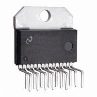
15-Lead TO-220 Molded Power Package
See NS Package Number TA15A
Order Number LMD18245T
Top View
2
Pin 12, SGND: Ground return node of all signal level circuits.
Pin 13, CS OUT: Output of the current sense amplifier. The
current sense amplifier sources 250 µA (typical) per ampere
of total forward current conducted by the upper two switches
of the power bridge.
Pin 14, DAC REF: Voltage reference input of the DAC. The
DAC provides an analog voltage equal to V
where D is the decimal equivalent (0–15) of the binary
number applied at M4 through M1.
Pin 15, OUT 2: Output node of the second half H-bridge.
X = don’t care
MONO is the output of the monostable.
BRAKE DIRECTION
H
L
L
L
L
TABLE 1. Switch Control Logic Truth Table
X
H
H
L
L
01187802
MONO
H
H
X
L
L
Source 1, Source 2
Source 2
Source 2, Sink 1
Source 1
Source 1, Sink 2
Active Switches
DAC REF
x D/16,
Related parts for LMD18245T/NOPB
Image
Part Number
Description
Manufacturer
Datasheet
Request
R

Part Number:
Description:
IC MOTOR DRIVER FULL BRIDGE 3A TO-220-15
Manufacturer:
National Semiconductor
Datasheet:

Part Number:
Description:
H-BRIDGE MOTOR DRIVER W/ PWM
Manufacturer:
National Semiconductor
Part Number:
Description:
Manufacturer:
National Semiconductor
Datasheet:

Part Number:
Description:
3a, 55v Dmos Full-bridge Motor Driver
Manufacturer:
National Semiconductor Corporation
Datasheet:
Part Number:
Description:
National Semiconductor [8-Bit D/A Converter]
Manufacturer:
National Semiconductor
Datasheet:
Part Number:
Description:
National Semiconductor [Media Coprocessor]
Manufacturer:
National Semiconductor
Datasheet:
Part Number:
Description:
Digitally Controlled Tone and Volume Circuit with Stereo Audio Power Amplifier, Microphone Preamp Stage and National 3D Sound
Manufacturer:
National Semiconductor
Datasheet:
Part Number:
Description:
Digitally Controlled Tone and Volume Circuit with Stereo Audio Power Amplifier, Microphone Preamp Stage and National 3D Sound
Manufacturer:
National Semiconductor
Datasheet:
Part Number:
Description:
AC97 Rev 2 Codec with Sample Rate Conversion and National 3D Sound
Manufacturer:
National Semiconductor
Part Number:
Description:
Manufacturer:
National Semiconductor
Datasheet:
Part Number:
Description:
Manufacturer:
National Semiconductor
Datasheet:
Part Number:
Description:
General Purpose, Low Voltage, Low Power, Rail-to-Rail Output Operational Amplifiers
Manufacturer:
National Semiconductor
Datasheet:
Part Number:
Description:
8-bit 20 MSPS flash A/D converter.
Manufacturer:
National Semiconductor
Datasheet:
Part Number:
Description:
Low Noise Quad Operational Amplifier
Manufacturer:
National Semiconductor
Datasheet: