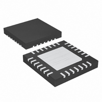
MAX6620ATI+ Maxim Integrated Products, MAX6620ATI+ Datasheet - Page 10

MAX6620ATI+
Manufacturer Part Number
MAX6620ATI+
Description
IC QUAD LIN FAN-SPD CTRLR 28TQFN
Manufacturer
Maxim Integrated Products
Datasheet
1.MAX6620ATI.pdf
(30 pages)
Specifications of MAX6620ATI+
Applications
Fan Controller
Number Of Outputs
4
Voltage - Supply
3 V ~ 5.5 V
Operating Temperature
-40°C ~ 125°C
Mounting Type
Surface Mount
Package / Case
28-TQFN Exposed Pad
Mounting Style
SMD/SMT
Lead Free Status / RoHS Status
Lead free / RoHS Compliant
Current - Output
-
Voltage - Load
-
Lead Free Status / Rohs Status
Lead free / RoHS Compliant
Quad Linear Fan-Speed Controller
A master initiates communication with a slave device by
issuing a START condition followed by a slave address
byte. As shown in Figure 5, the slave address byte con-
sists of 7 address bits and a read/write bit (R/W). When
idle, the MAX6620 continuously waits for a START con-
dition followed by its slave address. The first four bits
(MSBs) of the slave address have been factory pro-
grammed and are always 0101 and the seventh bit is 0.
Connect ADDR to GND or V
to program D2 and D1 of the slave address according
to Table 1.
Table 1. Slave Address Setting with
ADDR Pin
After receiving the address, the MAX6620 (slave)
issues an acknowledgement by pulling SDA low for one
clock cycle.
Single Read and Burst Read. A single read begins
with the bus master issuing a START condition followed
by the seven slave ID address bits and a zero (WR,
Figure 2), which is followed by an acknowledge bit (A)
from the slave corresponding to the slave ID. Next, the
master sends out an 8-bit register address, which is
also followed by an acknowledge bit from the slave.
The bus master issues another START condition and
the same seven slave ID address bits followed by a one
(RD, Figure 2), with the slave producing an acknowl-
edge bit. The slave then sends out the 8-bit data corre-
sponding to the register address previously written by
the master. The bus master sends back a not-acknowl-
edge bit (A). This completes the single read process
and a STOP condition is issued by the bus master.
Figure 5. MAX6620 Slave Address Byte
10
ADDR CONNECTION
______________________________________________________________________________________
Unconnected
SDA
SCL
GND
V
CC
S
0
Data Byte (Read and Write)
CC
1
0x50
0x52
0x54
HEX
, or leave it unconnected
SLAVE ADDRESS
1
2
Slave Address
0101 000
0101 010
0101 100
BINARY
0
3
1
4
In a burst read, the process is the same as a single
read except that the bus master issues an acknowl-
edge bit after each byte transmitted by the slave. After
each acknowledge bit, the register address increments
by one, and the data from the next register is transmit-
ted by the slave. The process continues, with data
reads followed by acknowledges. After the register with
the highest address is read, the register pointer rolls
over to point to the first register. To terminate a burst
read, the bus master issues a STOP condition.
Single Write and Burst Write. A single write begins
with the bus master issuing a START condition followed
by the seven slave ID address bits and a zero (WR,
Figure 2), which is followed by an acknowledge bit (A)
from the slave corresponding to the slave ID. Next, the
master sends out an 8-bit register address, which is
also followed by an acknowledge bit from the slave.
After the acknowledge bit, 8-bit data is written to the
register, and the slave issues a third acknowledgement.
A STOP condition is issued by the bus master to com-
plete the single write process.
In a burst write, the process is similar to a single write
except that the master does not issue a STOP condition
immediately after the first byte has been written. After
the first write is completed, the slave issues an
acknowledge bit, the register address increments by
one, and the data to be written to the next register is
transmitted by the master. The process continues, with
data writes followed by acknowledges. After the regis-
ter with the highest available address is written, the reg-
ister pointer rolls over to point to the first register. To
terminate a burst write, the bus master issues a STOP
condition.
The MAX6620 uses external pass transistors to power
the fans. DACOUT1–DACOUT4 adjust the power-
supply voltage for each fan by driving the base of a
PNP bipolar transistor, or the gate of a p-MOSFET. The
resulting fan-supply voltage is fed back to DACFB_.
This closes the voltage feedback loop. The system
power supply for the output devices is V
D2
5
D1
6
0
7
R/W
8
ACKNOWLEDGE
A
9
FAN
Fan Drive
. V
FAN
is


