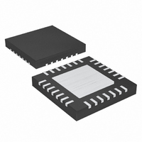
MAX6620ATI+ Maxim Integrated Products, MAX6620ATI+ Datasheet - Page 9

MAX6620ATI+
Manufacturer Part Number
MAX6620ATI+
Description
IC QUAD LIN FAN-SPD CTRLR 28TQFN
Manufacturer
Maxim Integrated Products
Datasheet
1.MAX6620ATI.pdf
(30 pages)
Specifications of MAX6620ATI+
Applications
Fan Controller
Number Of Outputs
4
Voltage - Supply
3 V ~ 5.5 V
Operating Temperature
-40°C ~ 125°C
Mounting Type
Surface Mount
Package / Case
28-TQFN Exposed Pad
Mounting Style
SMD/SMT
Lead Free Status / RoHS Status
Lead free / RoHS Compliant
Current - Output
-
Voltage - Load
-
Lead Free Status / Rohs Status
Lead free / RoHS Compliant
Figure 3. I
Figure 4. I
The master initiates a transmission with a START condi-
tion (S), a high-to-low transition on SDA with SCL high.
The master terminates a transmission with a STOP condi-
tion (P), a low-to-high transition on SDA while SCL is high
(Figure 3). The STOP condition frees the bus and places
all devices in F/S mode (Figure 1). Use a repeated
START condition (Sr) in place of a STOP condition to
leave the bus active and in its current timing mode.
Successful data transfers are acknowledged with an
acknowledge bit (A) or a not-acknowledge bit (A). Both
the master and the MAX6620 (slave) generate acknowl-
A = START CONDITION
B = MSB OF ADDRESS CLOCKED INTO SLAVE
C = LSB OF ADDRESS CLOCKED INTO SLAVE
D = R/W BIT CLOCKED INTO SLAVE
E = SLAVE PULLS SMBDATA LINE LOW
SCL
SDA
A = START CONDITION
B = MSB OF ADDRESS CLOCKED INTO SLAVE
C = LSB OF ADDRESS CLOCKED INTO SLAVE
D = R/W BIT CLOCKED INTO SLAVE
SCL
SDA
2
2
t
SU:STA
C Write Timing Diagram
C Read Timing Diagram
t
SU:STA
A
A
t
t
HD:STA
HD:STA
_______________________________________________________________________________________
t
t
LOW
LOW
B
B
START and STOP Conditions
t
t
HIGH
HIGH
Quad Linear Fan-Speed Controller
t
t
SU:DAT
SU:DAT
F = ACKNOWLEDGE BIT CLOCKED INTO MASTER
G = MSB OF DATA CLOCKED INTO MASTER
H = LSB OF DATA CLOCKED INTO MASTER
I = MASTER PULLS DATA LINE LOW
Acknowledge Bits
C
C
E = SLAVE PULLS SMBDATA LINE LOW
F = ACKNOWLEDGE BIT CLOCKED INTO MASTER
G = MSB OF DATA CLOCKED INTO SLAVE
H = LSB OF DATA CLOCKED INTO SLAVE
D
D
E
E
F
F
edge bits. To generate an acknowledge, the receiving
device must pull SDA low before the rising edge of the
acknowledge-related clock pulse (9th pulse), and keep it
low during the high period of the clock pulse (Figure 4).
To generate a not acknowledge, the receiver allows
SDA to be pulled high before the rising edge of the
acknowledge-related clock pulse, and leaves it high
during the high period of the clock pulse. Monitoring
the acknowledge bits allows for detection of unsuc-
cessful data transfers. An unsuccessful data transfer
happens if a receiving device is busy or if a system
fault has occurred. In the event of an unsuccessful data
transfer, the master should reattempt communication at
a later time.
t
HD:DAT
G
G
J = ACKNOWLEDGE CLOCKED INTO SLAVE
K = ACKNOWLEDGE CLOCK PULSE
L = STOP CONDITION
M = NEW START CONDITION
H
H
I = MASTER PULLS DATA LINE LOW
J = ACKNOWLEDGE CLOCKED INTO SLAVE
K = ACKNOWLEDGE CLOCK PULSE
L = STOP CONDITION
M = NEW START CONDITION
I
I
J K
J
K
t
SU:STO
t
SU:STO
L
L
t
BUF
t
BUF
M
M
9


