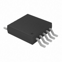
TC655EUNTR Microchip Technology, TC655EUNTR Datasheet - Page 11

TC655EUNTR
Manufacturer Part Number
TC655EUNTR
Description
IC PWM FAN SPEED CONTRLR 10-MSOP
Manufacturer
Microchip Technology
Type
High Speed PWM Controllerr
Datasheet
1.TC654EUN.pdf
(36 pages)
Specifications of TC655EUNTR
Applications
Fan Controller, Brushless (BLDC)
Number Of Outputs
1
Voltage - Supply
3 V ~ 5.5 V
Operating Temperature
-40°C ~ 85°C
Mounting Type
Surface Mount
Package / Case
10-MSOP, Micro10™, 10-uMAX, 10-uSOP
Output Current
5 mA
Operating Supply Voltage
3 V to 5.5 V
Maximum Operating Temperature
+ 85 C
Minimum Operating Temperature
- 40 C
Mounting Style
SMD/SMT
Lead Free Status / RoHS Status
Lead free / RoHS Compliant
Current - Output
-
Voltage - Load
-
Lead Free Status / Rohs Status
Lead free / RoHS Compliant
Available stocks
Company
Part Number
Manufacturer
Quantity
Price
Company:
Part Number:
TC655EUNTR
Manufacturer:
MICROCHIP
Quantity:
12 000
Part Number:
TC655EUNTR
Manufacturer:
MICROCHIP/微芯
Quantity:
20 000
4.3
Often overlooked in fan speed control is the actual
startup control period. When starting a fan from a non-
operating condition (fan speed is zero RPM), the
desired PWM duty cycle or average fan voltage can not
be applied immediately. Since the fan is at a rest posi-
tion, the fan’s inertia must be overcome to get it started.
The best way to accomplish this is to apply the full rated
voltage to the fan for one second. This will ensure that
in all operating environments, the fan will start and
operate properly.
The TC654 and TC655 devices implement this fan con-
trol feature without any user programming. During a
power up or release from shutdown condition, the
TC654 and TC655 devices force the V
100% duty cycle, turning the fan full on for one second
(C
TC654/TC655 devices will look to see if SMBus or V
control has been selected in the Configuration Register
(DUTYC bit 5<0>). Based on this register, the device
will choose which input will control the V
Duty cycle control based on V
V
is connected to the V
default to a duty cycle of 39.33%. This sequence is
shown in Figure 4-4. This integrated one second star-
tup feature will ensure the fan starts up every time.
FIGURE 4-4:
4.4
As previously discussed, the TC654 and TC655
devices operate with a fixed PWM frequency. The fre-
quency of the PWM drive output (V
capacitor at the C
pin, the typical drive frequency is 30 Hz. This frequency
can be raised, by decreasing the capacitor value, or
lowered, by increasing the capacitor value. The rela-
tionship between the capacitor value and the PWM fre-
IN
Default PWM: 39.33%
2002 Microchip Technology Inc.
F
control is selected and the V
= 1 µF). Once the one second period is over, the
PWM Drive Frequency (C
Fan Startup
YES
Power Up or Release
F
One Second Pulse
V
pin. With a 1 µF capacitor at the C
Select SMBus
Cycle Control
IN
IN
from SHDN
V
PWM Duty
IN
Power-up Flow Chart.
pin), then the TC654/TC655 will
Open?
NO
NO
IN
IN
is the default state. If
pin is open (nothing
YES
SMBus PWM Duty
OUT
Cycle Control
OUT
OUT
) is set by a
F
)
output to a
duty cycle.
IN
F
quency is linear. If a frequency of 15 Hz is desired, a
capacitor value of 2.0 µF should be used. The fre-
quency should be kept in the range of 15 Hz to 35 Hz.
See Section 7.2 for more details.
4.5
The duty cycle of the V
controlled by either the V
Duty-Cycle Register, which is accessible via the
SMBus interface. The control method is selectable via
DUTYC (bit 5<0>) of the Configuration Register. The
default state is for V
and the V
to 39.33%. The duty cycle control method can be
changed at any time via the SMBus interface.
V
1.62 V to 2.6 V (typical) at this pin commands a 30% to
100% duty cycle on the V
voltage at V
cycle will not go below 30%. The relationship between
the voltage at V
Figure 4-5.
FIGURE 4-5:
Voltage (Typical).
For the TC655 device, if the voltage at V
2.6 V (typical) level, an over temperature fault indica-
tion will be given by asserting a low at the FAULT output
and setting OTF (bit 5<X>) in the Status Register to a
‘1’.
A thermistor network or any other voltage output ther-
mal sensor can be used to provide the voltage to the
V
ally be thought of as a temperature. For example, the
circuit shown in Figure 4-6 represents a typical solution
for a thermistor based temperature sensing network.
See Section 7.3 for more details.
IN
IN
input. The voltage supplied to the V
is an analog input pin. A voltage in the range of
100
90
80
70
60
50
40
30
20
10
0
Duty Cycle Control (V
Cycle Register)
IN
1
pin is open, the PWM duty cycle will default
IN
1.2
falls below the 1.62 V level, the duty
IN
1.4
and the PWM duty cycle is shown in
TC654/TC655
IN
1.6
control. If V
Input Voltage (V
PWM Duty Cycle vs. V
OUT
OUT
IN
1.8
analog input pin or by the
PWM drive signal can be
output, respectively. If the
2
IN
2.2
IN
control is selected
DS21734A-page 11
)
IN
IN
IN
2.4
and Duty-
pin can actu-
exceeds the
2.6
IN
2.8


