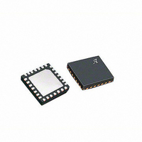
A4988SETTR-T Allegro Microsystems Inc, A4988SETTR-T Datasheet

A4988SETTR-T
Specifications of A4988SETTR-T
Available stocks
Related parts for A4988SETTR-T
A4988SETTR-T Summary of contents
Page 1
DMOS Microstepping Driver with Translator Features and Benefits ▪ Low R outputs DS(ON) ▪ Automatic current decay mode detection/selection ▪ Mixed and Slow current decay modes ▪ Synchronous rectification for low power dissipation ▪ Internal UVLO ▪ Crossover-current protection ▪ ...
Page 2
... PWM operation. Internal circuit protection includes: thermal shutdown with hysteresis, undervoltage lockout (UVLO), and crossover-current protection. Special power-on sequencing is not required. Selection Guide Part Number A4988SETTR-T 28-contact QFN with exposed thermal pad Absolute Maximum Ratings Characteristic Load Supply Voltage Output Current ...
Page 3
A4988 VREG VDD Current Regulator REF DAC PWM Latch Blanking Mixed Decay STEP DIR RESET Control Translator MS1 Logic MS2 MS3 PWM Latch ENABLE Blanking Mixed Decay SLEEP DAC V REF DMOS Microstepping Driver with Translator Functional Block Diagram 0.22 ...
Page 4
A4988 ELECTRICAL CHARACTERISTICS Characteristics Output Drivers Load Supply Voltage Range Logic Supply Voltage Range Output On Resistance Body Diode Forward Voltage Motor Supply Current Logic Supply Current Control Logic Logic Input Voltage Logic Input Current Microstep Select Logic Input Hysteresis ...
Page 5
A4988 THERMAL CHARACTERISTICS Characteristic Package Thermal Resistance *Additional thermal information available on Allegro Web site. DMOS Microstepping Driver with Translator Symbol Test Conditions* R Four-layer PCB, based on JEDEC standard θJA Power Dissipation versus Ambient Temperature 4.00 3.50 3.00 2.50 ...
Page 6
A4988 STEP MS1, MS2, MS3, RESET, or DIR STEP minimum, HIGH pulse width STEP minimum, LOW pulse width Setup time, input change to STEP Hold time, input change to STEP Figure 1. Logic Interface Timing Diagram Table 1. Microstepping Resolution ...
Page 7
A4988 The A4988 is a complete microstepping Device Operation. motor driver with a built-in translator for easy operation with minimal control lines designed to operate bipolar stepper motors in full-, half-, quarter-, eighth, and sixteenth-step modes. The currents ...
Page 8
A4988 Slow Mixed Decay Decay Missed Step Voltage on ROSC terminal 2 V/div. Step input 10 V/div. Figure 2. Missed steps in low-speed microstepping I 500 mA/div. LOAD Step input 10 V/div. Figure 3. Continuous stepping using automatically-selected mixed stepping ...
Page 9
A4988 tion of current flow in each winding. The size of the increment is determined by the combined state of the MSx inputs. (DIR). This determines the direction of rota- Direction Input tion of the motor. Changes to this input ...
Page 10
A4988 This internally-generated voltage is used (VREG) REG operate the sink-side FET outputs. The nominal output voltage of the VREG terminal The VREG pin must be decoupled with a 0.22 μF ceramic capacitor to ...
Page 11
A4988 V STEP 100.00 70.71 I OUT 0 –70.71 –100.00 I OUT Symbol I Figure 7. Current Decay Modes Timing Chart DMOS Microstepping Driver with Translator See Enlargement A Enlargement PEAK Characteristic t Device fixed off-time ...
Page 12
A4988 Layout. The printed circuit board should use a heavy ground- plane. For optimum electrical and thermal performance, the A4988 must be soldered directly onto the board. Pins 3 and 18 are internally fused, which provides a path for enhanced ...
Page 13
A4988 VDD VBB 8 V GND GND V BB VREG SENSE 10 V GND DMOS Microstepping Driver with Translator Pin Circuit Diagrams GND PGND GND MS1 MS2 MS3 V REG DIR VREF ROSC DMOS SLEEP Parasitic GND ...
Page 14
A4988 STEP 100.00 70.71 Phase 1 I OUT1A 0.00 Direction = H (%) –70.71 –100.00 100.00 70.71 Phase 2 I OUT2A 0.00 Direction = H (%) –70.71 –100.00 Figure 8. Decay Mode for Full-Step Increments STEP Phase 1 I OUT1A ...
Page 15
A4988 STEP 100.00 92.39 83.15 70.71 55.56 38.27 Phase 1 19.51 I OUT1A 0.00 Direction = H –19.51 (%) –38.27 –55.56 –70.71 –83.15 –92.39 –100.00 100.00 92.39 83.15 70.71 55.56 38.27 Phase 2 19.51 I OUT2B 0.00 Direction = H ...
Page 16
A4988 STEP 100.00 95.69 88.19 83.15 77.30 70.71 63.44 55.56 47.14 38.27 29.03 19.51 Phase 1 9.8 I OUT1A 0.00 Direction = H –9.8 (%) –19.51 –29.03 –38.27 –47.14 –55.56 –63.44 –70.71 –77.30 –83.15 –88.19 –95.69 –100.00 100.00 95.69 88.19 ...
Page 17
A4988 Table 2. Step Sequencing Settings Home microstep position at Step Angle 45º; DIR = H Phase 1 Full Half 1/4 1/8 1/16 Current Step Step Step Step Step [% I tripMax ] # # # # # 1 1 ...
Page 18
A4988 Terminal List Table Name CP1 CP2 VCP VREG MS1 MS2 MS3 ¯ R ¯ ¯ E ¯ ¯ S ¯ ¯ E ¯ ¯ T ¯ ROSC ¯ S ¯ ¯ L ¯ ¯ E ¯ ¯ E ¯ ...
Page 19
A4988 ET Package, 28-Pin QFN with Exposed Thermal Pad 29X 0.08 C +0.05 0.25 –0.07 0.73 MAX DMOS Microstepping Driver with Translator 5.00 ±0.15 1. 5.00 ±0.15 C SEATING PLANE ...
Page 20
A4988 Revision History Revision Rev. 2 Copyright ©2009-2011, Allegro MicroSystems, Inc. Allegro MicroSystems, Inc. reserves the right to make, from time to time, such de par tures from the detail spec tions as may be required to ...


