MC3PHACVDWE Freescale Semiconductor, MC3PHACVDWE Datasheet - Page 6
MC3PHACVDWE
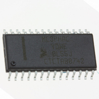
Manufacturer Part Number
MC3PHACVDWE
Description
IC MOTOR CONTROLLER 28-SOIC
Manufacturer
Freescale Semiconductor
Datasheet
1.MC3PHACVFAE.pdf
(36 pages)
Specifications of MC3PHACVDWE
Applications
AC Motor Controller, 3 Phase
Number Of Outputs
1
Voltage - Supply
4.5 V ~ 5.5 V
Operating Temperature
-40°C ~ 105°C
Mounting Type
Surface Mount
Package / Case
28-SOIC (7.5mm Width)
Processor Series
MC3PHAC
Core
HC08
Data Bus Width
8 bit
Program Memory Type
Flash
Program Memory Size
8 KB
Data Ram Size
256 KB
Interface Type
SCI
Maximum Clock Frequency
8.2 MHz
Number Of Programmable I/os
14
Number Of Timers
2
Maximum Operating Temperature
+ 85 C
Mounting Style
SMD/SMT
Minimum Operating Temperature
- 40 C
On-chip Adc
10 bit, 4 Channel
Lead Free Status / RoHS Status
Lead free / RoHS Compliant
Current - Output
-
Voltage - Load
-
Lead Free Status / Rohs Status
Details
Available stocks
Company
Part Number
Manufacturer
Quantity
Price
Company:

Part Number:
MC3PHACVDWE
Manufacturer:
NSC
Quantity:
1 430


Pin Descriptions
Pin Descriptions
Table 2
28-pin packages (see
6
Number
Pin
10
11
12
13
14
15
16
1
2
3
4
5
6
7
8
9
is a pin-by-pin functional description of the MC3PHAC. The pin numbers in the table refer to the
PWMPOL_BASEFREQ
PWMFREQ_RxD
PWM_W_TOP
PWM_W_BOT
PWM_U_TOP
PWM_U_BOT
PWM_V_TOP
PWM_V_BOT
Pin Name
PLLCAP
FAULTIN
RESET
OSC2
OSC1
V
V
V
DDA
REF
SSA
Figure
Table 2. MC3PHAC Pin Descriptions (Sheet 1 of 2)
MC3PHAC Monolithic Intelligent Motor Controller, Rev. 2
2).
Reference voltage input for the on-chip ADC. For best signal-to-noise
A logic 0 on this pin forces the MC3PHAC to its initial startup state. All
Provides power for the analog portions of the MC3PHAC, which include
Returns power for the analog portions of the MC3PHAC, which include
Oscillator output used as part of a crystal or ceramic resonator clock
Oscillator input used as part of a crystal or ceramic resonator clock
A capacitor from this pin to ground affects the stability and reaction time
Input which is sampled at specific moments during initialization to
PWM output signal for the top transistor driving motor phase U
PWM output signal for the bottom transistor driving motor phase U
PWM output signal for the top transistor driving motor phase V
PWM output signal for the bottom transistor driving motor phase V
PWM output signal for the top transistor driving motor phase W
PWM output signal for the bottom transistor driving motor phase W
A logic high on this input will immediately disable the PWM outputs. A
In standalone mode, this pin is an output that drives low to indicate the
performance, this pin should be tied to V
PWM outputs are placed in a high-impedance mode. Reset is a
bidirectional pin, allowing a reset of the entire system. It is driven low
when an internal reset source is asserted (for example, loss of clock or
low V
the internal clock generation circuit (PLL) and the ADC
the internal clock generation circuit (PLL) and the ADC
circuit.
circuit. Can also accept a signal from an external canned oscillator.
of the PLL clock circuit. Smaller values result in faster tracking of the
reference frequency. Larger values result in better stability. A value of
0.1 µF is typical.
determine the PWM polarity and the base frequency (50 or 60 Hz)
retry timeout interval will be initiated once this pin returns to a logic low
state.
parameter mux input pin is reading an analog voltage to specify the
desired PWM frequency. In PC master software mode, this pin is an
input which receives UART serial data.
DD
(1)
).
Pin Function
DDA
(analog).
Freescale Semiconductor
(1)
Related parts for MC3PHACVDWE
Image
Part Number
Description
Manufacturer
Datasheet
Request
R

Part Number:
Description:
Mc3phac Motor Control Unit
Manufacturer:
Freescale Semiconductor, Inc
Datasheet:
Part Number:
Description:
Manufacturer:
Freescale Semiconductor, Inc
Datasheet:
Part Number:
Description:
Manufacturer:
Freescale Semiconductor, Inc
Datasheet:
Part Number:
Description:
Manufacturer:
Freescale Semiconductor, Inc
Datasheet:
Part Number:
Description:
Manufacturer:
Freescale Semiconductor, Inc
Datasheet:
Part Number:
Description:
Manufacturer:
Freescale Semiconductor, Inc
Datasheet:
Part Number:
Description:
Manufacturer:
Freescale Semiconductor, Inc
Datasheet:
Part Number:
Description:
Manufacturer:
Freescale Semiconductor, Inc
Datasheet:
Part Number:
Description:
Manufacturer:
Freescale Semiconductor, Inc
Datasheet:
Part Number:
Description:
Manufacturer:
Freescale Semiconductor, Inc
Datasheet:
Part Number:
Description:
Manufacturer:
Freescale Semiconductor, Inc
Datasheet:
Part Number:
Description:
Manufacturer:
Freescale Semiconductor, Inc
Datasheet:
Part Number:
Description:
Manufacturer:
Freescale Semiconductor, Inc
Datasheet:
Part Number:
Description:
Manufacturer:
Freescale Semiconductor, Inc
Datasheet:
Part Number:
Description:
Manufacturer:
Freescale Semiconductor, Inc
Datasheet: